After receive all the data, we can arrange the production as below:
Step 1. BOM checking

Before assembly, our experienced engineers check your BOM (bill of materials). This makes sure that electronic components are okay for PCB assembly.
Step 2. Transferring PCBs from automatic loader to solder paste printing machine
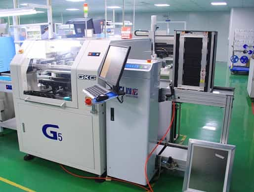
When bare PCB boards made at our PCB production base or sent from customers are brought to our PCBA factory, they are loaded on the automatic loader. Then the loader will transfer the PCBs into the solder paste printing machine
Step 3. Printing solder paste onto the PCBs
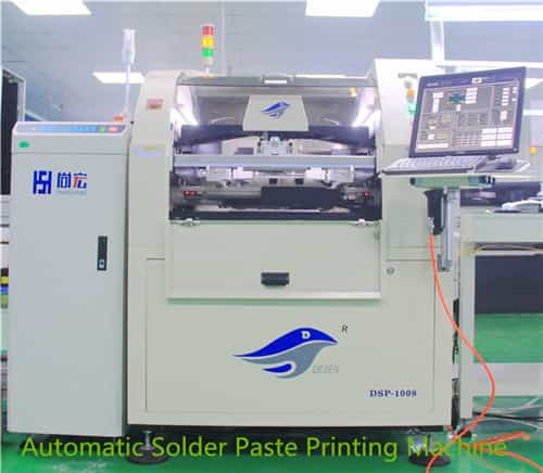
Inside the automatic solder paste printing machine, a customized SMT stencil is pre-set. Every PCB board is piled under the SMT stencil, and the scraper blade of the machine will print solder paste on pads of PCBs one by one. Normally, in PCBONLINE, we set the pressure by the blade at 3±0.5KG, its tangle of 60°, and its speed at 60±5mm/s. When the PCB is taken off the SMT stencil, the speed is 0.5±0.05mm/s, and the distance between the PCB and the stencil is set to be 1.0-1.5mm. Then the machine cleans the SMT stencil by drying it up.
Note: under 0°C to 10°C, solder paste is thick, and only under 22°C to 28°C when the solder paste is pasty can it be printed. If you DIY a PCBA, please keep your solder paste in the environment under 22°C to 28°C. At PCBONLINE, we store solder paste under 2° to 8°C in the cooler, and before using it for SMT assembly, we take it out and let it stand still for four hours to allow a gentle rise in temperature to 22°C to 28°C.
Step 4. Inspect thickness and shape of solder paste
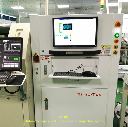
Standard solder paste thickness ranges from 0.09mm to 0.15mm, and the SMT stencil thickness has to be within the tolerance of ±0.03mm than the solder paste thickness. We use the SPI machine to inspect solder paste, and only if its thickness is in this range and its shape is qualified can we let the PCBs go to the next procedure. Some PCBs may require thinner or thicker solder paste, depending on the application requirements, and we will set the custom thickness range
Step 5. Placing small components onto the PCBs
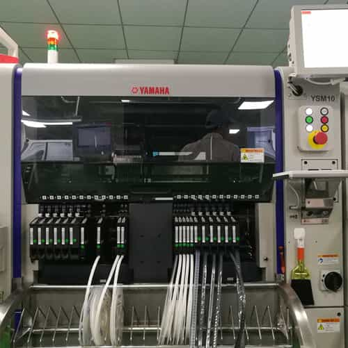
At this step, PCBs printed with solder paste are sent inside the high-speed mounter, and then small components are placed onto the corresponding pads of PCBs. The high-speed mounter runs extremely fast, and in seconds the PCBs are brought next into the functional mounter.
Step 6. Placing large components onto the PCBs
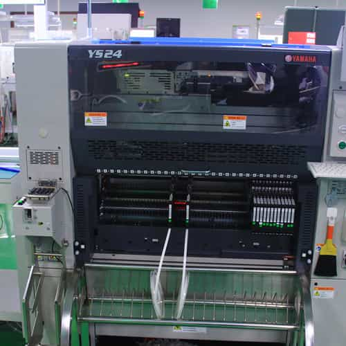
When PCBs mounted with small components come into the functional mounter, large components are placed onto them accurately
Step 7. Reflow soldering
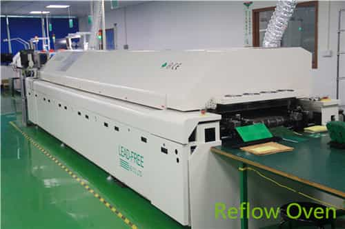
Reflow soldering is the most important step in a PCBA process. Your mounted PCBs are transferred by a conveyor belt moving horizontally with a uniform velocity through a reflowing oven. The reflowing oven has ten temperature zones. From the first to the ninth, temperature increases following the pre-set temperature curve, and solder paste melts on the pads. The tenth is a cooling zone, where solder paste sets. Then electronic components and pads on PCBs are connected tightly, and you are getting the PCBAs.
Note: The velocity of the conveyor and temperatures of the zones of the reflowing oven are not settled. They are set by experienced engineers in our PCBA factory, according to the application requirements. The melting point of the solder paste is 217°C.
Step 8. X-ray inspection and visual inspection
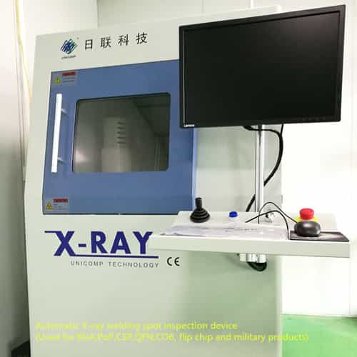
The mounted PCBs will be transferred into an X-ray machine to detect if there are any soldering defects, and then an experienced technician inspects some samples visually. The PCBs won’t go to the next step until everything is okay.
Step 9. Repeat step 2 to step 8 to mount components on the other side (optional)
After the above steps, your PCBs are mounted with components on one side, and usually, they will go to the next step. But some PCBs are designed to have two sides mounted with components. In this case, we will repeat steps from 2 to 8 to mount components on the other side.
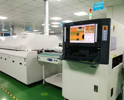
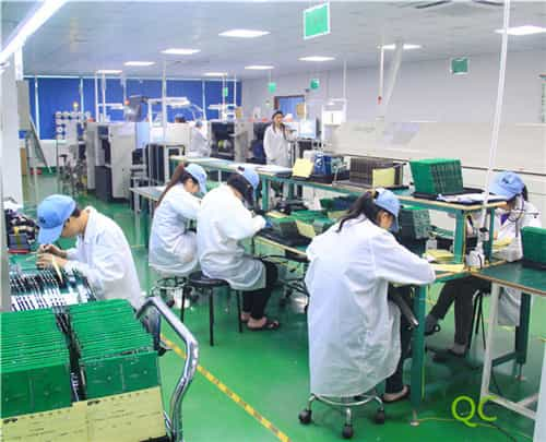
Step 10. AOI testing, visual inspection, and sampling inspection
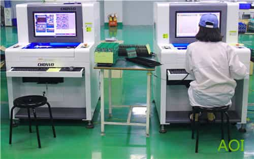
Unlike other PCB assembler whose AOI is only 2D-scanning, we use 3D-scanning. Any possible defects are noted on the screen, and our AOI operator checks them one by one and records if there are any real defects. The defective products will be picked out. Then another technician checks the PCBAs visually, and the samely, any defects will be recorded, and defective products will be picked out. Next, some PCBA samples will go through the sampling inspection in the testing area. All the defective products will be sent to be repaired, and after repairing, they are also separated from other PCBAs.
Step 11. Fit long legs of components through PCB holes using DIP
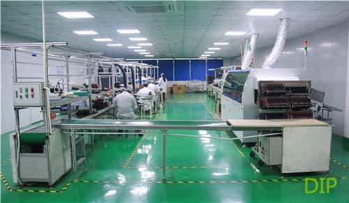
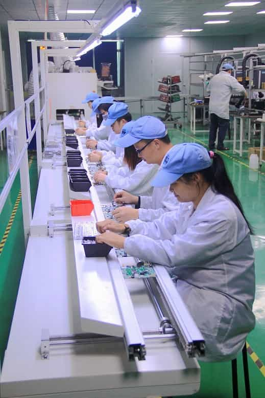
Some components with long legs can't be soldered on PCBs on an SMT assembly line, so the PCBAs are transferred to a THT (through-hole technology) assembly line. We use a DIP machine to insert the long legs through the holes of PCBs.
Step 12. Wave soldering
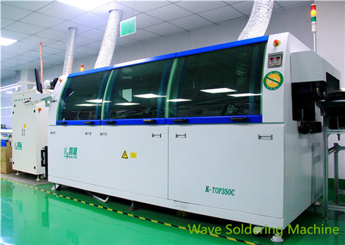
The long legs of components need to be soldered, and wave soldering is processed with two aims: fixing the components with PCBAs and using tin to fill the gap between long legs and PCBA holes to connect components electrically. The soldering side of PCBAs will soak in melting tin through the wave soldering oven, and then, we will use a cutter to trim the component legs to be 1mm to 2mm.
Step 13. Touch-up, cleaning, and visual inspection
After the wave soldering, there may be some defects such as soldering holes and insufficient tin plating, so we need to fix them by touch-up. A well-trained technician inspects the PCBAs carefully and uses a soldering iron to fill the board surface with tin. After this, if there are extra tin on the board, the technician will use flux to remove it in case of a short-circuit. Then, the technician inspects the PCBAs again.
Step 14. IC-programming downloading (optional)
IC-programming means downloading programs into integrated circuits. Sometimes, the ICs sent from customers are already downloaded with their own programs, and we will pass this step. A technician connects the IC connector to the computer using a USB cable and clicks the download button to install programs on the IC
Step 15. Functional testing using a PCB tester
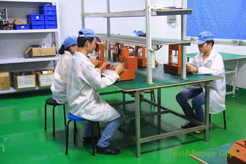
A technician fits the PCBA on a PCB tester, charges with electricity, and checks the current, voltage, and other parameters depending on the application use. If the product has a screen, he/she will also check the screen brightness and whether there is flickering and flashing.
Step 16. Aging testing
Aging tests means we power the PCBA/product on to let it work at the room temperature and a constant higher or lower temperature for a period (usually 12 hours respectively), and then inspect whether the PCBA/product is in good condition. If the PCBA work normally after the aging test, we assemble the product.