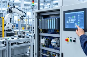
Printed circuit boards (PCBs) serve as the “skeleton and veins” of electronic products, and the quality and efficiency of their assembly (PCBA) directly determine the performance and reliability of the final product. With the widespread application of high-density interconnects (HDI), micro-components (such as 01005 and 008004 packages), and complex packages (such as SiP and BGA), the traditional rule-based PCB assembly model, relying on manual experience and inspection, is facing severe challenges, including long production line adjustment cycles, bottlenecks in defect rate control, high false alarm rates in defect detection, and difficulties in optimizing process parameters in real time.
Deeply integrating artificial intelligence (AI) technology into the entire lifecycle of PCB assembly—from design process development (DFM) to component procurement, surface mount technology (SMT), soldering temperature control, optical and X-ray inspection (AOI/AXI), and after-sales fault traceability—has become a core path for the electronics manufacturing industry to achieve intelligent transformation and lean production.
I. Bottlenecks in Traditional PCB Assembly Processes and Entry Points for AI Integration
Before discussing how to integrate AI technology, it is necessary to clarify the pain points in traditional PCB assembly processes and the cost reduction and efficiency improvement logic of AI technology in each stage.
| Assembly Stage / Process | Traditional Pain Points | AI Integration & Entry Point | Expected Benefits |
| Design for Manufacturability (DFM) | Relies on manual engineering experience; rule-based libraries lag in updates, making it easy to miss high-density layout defects | AI deep learning models simulate placement and soldering processes, automatically predicting assembly interference and soldering defects | Lower design rework rate, shortened NPI (New Product Introduction) cycle |
| Solder Paste Printing (SPI) | Parameter settings rely heavily on technician experience; solder paste volume and shape are vulnerable to ambient temperature and humidity fluctuations | Machine learning-based intelligent closed-loop control, real-time prediction and fine-tuning of stencil cleaning, squeegee pressure, and speed | Reduction of source soldering defects such as bridging, insufficient solder, and tombstoning |
| SMT Pick & Place | Low recognition rate for odd-form/custom components; nozzle suction status is difficult to monitor in real-time, resulting in high rates of flying lines or dropped components (component wastage) | AI computer vision recognizes component posture and deformation; reinforcement learning optimizes nozzle trajectories and material scheduling | Enhanced placement precision, reduced component wastage rate, and shorter placement cycle time |
| Reflow Soldering | Temperature profile configuration relies on trial and error; differences in thermal capacity across sections of complex boards easily lead to cold solder joints | Thermodynamic digital twins + algorithms predict optimal parameters for heating zones, dynamically adjusting the reflow profile in real-time | Reduced thermal stress deformation, enhanced solder joint reliability |
| Inspection & Quality Control (AOI/AXI) | Based on geometric feature matching, with extremely high false alarm rates, requiring extensive manual secondary review | CNN/Transformer deep learning image segmentation and classification combined with multi-modal data for precision judgment | Reduction of false alarm rates by over 90%, lower manual review labor costs |
| Process Traceability & Equipment Maintenance | Lagging response to anomalies; maintenance relies on “reactive maintenance” or “scheduled maintenance,” causing heavy downtime losses | IoT and predictive maintenance (PdM) models for real-time monitoring of equipment vibration, current, and wear status | Reduction of unplanned downtime, extended equipment lifespan |
II. Core Architecture and Technical Implementation Path of AI Integration in PCB Assembly
The integration of AI technology in PCB assembly is not an isolated application of algorithms, but rather a construction of a technical system based on “data acquisition – intelligent decision-making – closed-loop feedback.”
Manufacturing-Side Data Infrastructure Construction (The Soil for AI)
Equipment Networking and Data Standardization: Based on the IPC-HERMES-9852 and IPC-CFX (Connected Factory Exchange) standards, communication barriers between SPI, pick-and-place machines, reflow soldering, AOI, and MES systems are broken down to achieve real-time acquisition of millisecond-level data (including images, temperature, pressure, vibration, speed, and electrical parameters).
Multimodal Data Fusion: CAD/ODB++ data from the design end, sensor data from the production end, and high-resolution image data from the inspection end are uniformly mapped to a digital twin model, providing labeled data for AI model training.
Specific Integration Mechanisms of AI Models in Key Assembly Processes
AI + DFM/DFA: Intelligent Assembly Feasibility Prediction
During the PCB design phase, AI uses deep learning to construct an assemblability prediction model based on assembly data from tens of thousands of historical boards and a soldering defect database. The algorithm can automatically identify thermal barrier effects between high-density components and pin-pad fit tolerances, providing real-time modification suggestions in the design software to intercept design defects before manufacturing.
AI + Solder Paste Printing (SPI): Real-time Closed-Loop Control of Process Parameters
Solder paste printing defects account for over 60% of total SMT defects. With AI integration, the SPI inspection system can not only detect the volume, area, and height of solder paste but also feed the measurement data back to the printer’s AI control module in real time. Machine learning algorithms dynamically adjust squeegee pressure, printing speed, and demolding distance based on changes in ambient temperature and humidity and the rheological properties of the solder paste, achieving adaptive fine-tuning of the printing process.
AI + Surface Mount Recognition and Path Planning: Reinforcement Learning Improves Mounting Efficiency
For BGA, QFN, and irregularly shaped electronic devices, traditional CCD image algorithms struggle to accurately locate irregular pins or surface damage. By introducing convolutional neural networks (CNN) and Transformer architecture, the vision system can achieve micron-level mounting positioning and defect detection even at high speeds. Meanwhile, reinforcement learning algorithms are used to globally solve the nozzle allocation, material station layout, and motion trajectory of multi-head pick-and-place machines, significantly shortening the placement cycle.
AI + Reflow Soldering: Thermodynamic Digital Twin and Temperature Curve Optimization
Different board thicknesses, copper foil densities, and component layouts result in vastly different heat absorption rates during reflow soldering. AI combines finite element analysis (FEA) with thermodynamic data to establish a heat conduction model within the reflow oven. The system only needs to input the PCB’s CAD data and physical characteristics; the AI algorithm can calculate the optimal temperature zone settings (preheating, wetting, reflow, cooling) within seconds and adjust the heating power in real time based on feedback from board temperature sensors during production, ensuring that the IMC (intermetallic compound) thickness of each solder joint reaches the optimal level.
AI + AOI/AXI: Deep Learning Reshapes Defect Detection Accuracy
Traditional rule-based AOI heavily relies on manually set thresholds and is easily affected by solder joint gloss and PCB surface color fluctuations.
Image Segmentation and Classification: AI AOI employs semantic segmentation algorithms such as Mask R-CNN to accurately delineate solder joints, component bodies, and pad outlines, effectively distinguishing defects such as “tombstone,” “bridging,” “cold solder joints,” “misalignment,” and “voids.”
Few-Shot Learning and Generative AI: Addressing the scarcity of defect samples in New Product Injection (NPI), GAN (Generative Adversarial Network) or diffusion models are used to generate realistic defect images, improving the model’s generalization ability under extreme defect conditions.
Automatic Judgment and Reduced Manpower for Re-inspection: The AI model reduces the false positive rate to an extremely low level. The system only pushes a very small number of difficult samples with ambiguous probabilities to the manual review interface, achieving over 90% unmanned automated quality control.
III. Challenges and Countermeasures for Implementing AI-Integrated PCB Assembly
Data Quality and Sample Bias Issues
Challenge: Industrial field defect data is extremely scarce (yield rates are typically above 99%), and a severe lack of negative samples can lead to overfitting of the AI model.
Strategy: Deploy transfer learning and unsupervised anomaly detection algorithms to allow the model to “learn what is normal,” thereby automatically alerting to any foreign objects or welding patterns deviating from normal shapes.
Real-time Performance and Edge Computing Bottlenecks
Challenge: SMT production line placement speeds are extremely high (a single placement cycle takes only tens of milliseconds), and cloud inference latency cannot meet real-time control requirements.
Strategy: Adopt a “cloud training + edge deployment (Edge AI)” architecture. Deploy the quantized and lightweight AI model on edge computing nodes on the production line (such as GPU/NPU-based industrial PCs) to achieve sub-millisecond inference response.
Industrial Standards and System Integration Compatibility
Challenge: The factory contains both new and old equipment with heterogeneous communication protocols, making heterogeneous system integration difficult.
Strategy: Rely on the IPC-CFX standard to unify data interfaces and build modular AI microservices, reducing dependence on specific equipment hardware and enabling smooth upgrades.
IV. Summary and Future Outlook
The integration of AI technology with PCB assembly is essentially a process of shifting manufacturing experience from “human senses and memory” to “algorithm models and data flow.” By permeating every sub-node of DFM design, SMT placement, soldering temperature control, and AOI inspection, electronics manufacturing companies can significantly improve flexible manufacturing capabilities, reduce production losses, and achieve a true global quality closed loop.
In the future, with the further maturation of Large Language Models (LLM) and industrial multimodal agents, PCB assembly will evolve into a “Dark Factory” model characterized by “self-perception, self-diagnosis, and self-optimization.” AI technology will also transform from a simple “assistant quality control tool” into the “core brain driving the fully autonomous operation of the production line.”