
Top-Tier PCB Manufacturing & Fabrication Services
From 1 to 64 layers with advanced HDI, ultra-fine lines, and turnkey delivery backed by ISO certification.
Advanced Fabrication Capabilities & Tolerances
1–64 Layers
Advanced 18L Any-Layer HDI PCB
3–6 mil Microvias
Blind, Buried & Laser-Formed Holes
40:1 Aspect Ratio
±5% Precision Impedance Control
IPC & IATF 16949
ISO 9001/14001/13485 & UL Certified
Leading Precision PCB Manufacturing Partner in China
Featured Services

Quick-Turn PCB Prototyping
Accelerate your product time-to-market with fast turnaround delivery for prototypes and small-to-medium batch production runs.

Advanced Multilayer & Rigid PCBs
High-precision manufacturing supporting 1 to 64 layers with stringent impedance control, strict dielectric thickness, and high reliability.
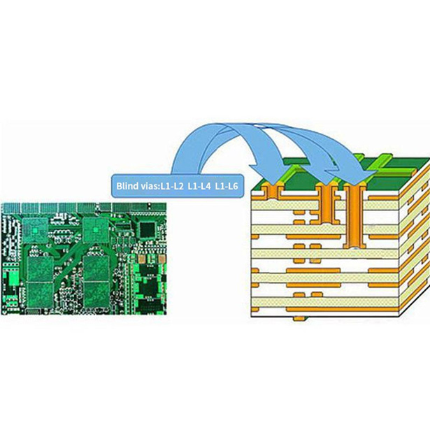
High-Density Interconnect (HDI)
State-of-the-art 18L any-layer designs leveraging 3 to 6 mil laser-formed microvias for compact, high-performance electronics.
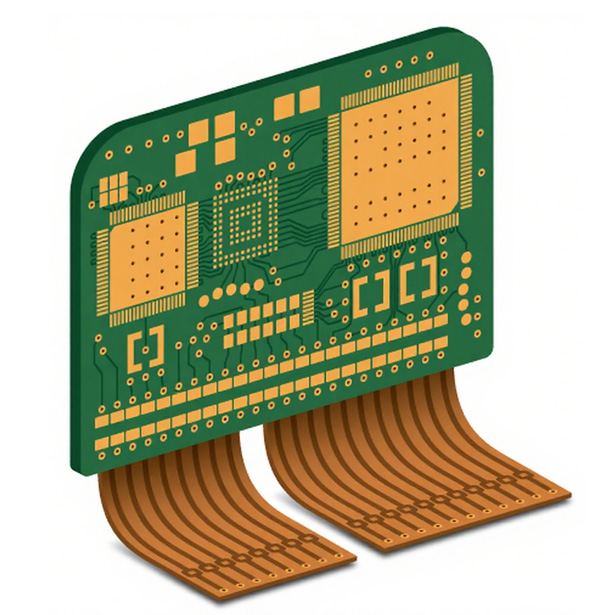
Flex & Rigid-Flex Solutions
Durable flexible and rigid-flex printed circuit boards engineered to withstand dynamic bending and complex spatial constraints.
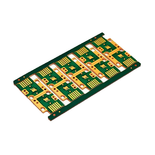
Heavy Copper & Specialty PCBs
Robust manufacturing capabilities supporting up to 28 oz heavy copper, high-frequency materials, and extreme aspect ratios.
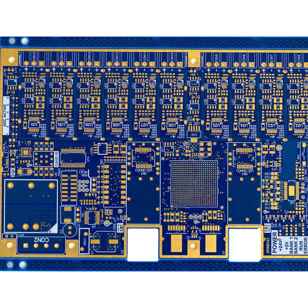
Premium Surface Finishes
Full suite of finishes including ENIG, ENEPIG, immersion silver, and OSP, backed by strict IPC and ISO quality standards.
Why Partner With Us for Advanced PCB Manufacturing?
As a premier China-based PCB manufacturing specialist, backed by ISO-certified smart factory capabilities, we deliver highly reliable bare PCBs engineered for high-end, tier-one applications requiring exceptional thermal performance, stringent signal integrity, and high-density designs in space-constrained environments.
From DFM engineering and process optimization to production and global logistics, we provide end-to-end manufacturing support. Our advanced production capabilities cover 1- to 64-layer rigid, flex, rigid-flex, and Any-Layer HDI PCBs, with precision manufacturing capabilities including 1.8 mil (approx. 0.045 mm) fine-line features, 3 mil (approx. 0.075 mm) laser-drilled microvias, and heavy copper up to 28 oz. We also offer a comprehensive range of surface finishes, including ENIG, ENEPIG, Immersion Silver, and OSP, delivering consistent mechanical integrity, electrical reliability, and long-term performance for demanding applications.
- Laser Direct Imaging (LDI)
- Controlled Dielectric Thickness
- Extreme Aspect Ratio Support
- Up to 28 oz Heavy Copper
- High-Frequency Materials (Rogers/Isola)
- Full-Spectrum Surface Finishes
- 100% Flying Probe & AOI Testing
- RoHS & REACH Compliant Production
- Rigid-Flex & Flex PCB Capability
- Quick-Turn Prototyping & Mass Production
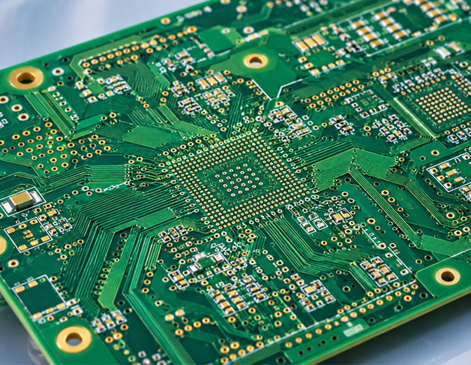
Industries We Serve
Advanced Precision PCB Manufacturing Engineered for Demanding Global Industries
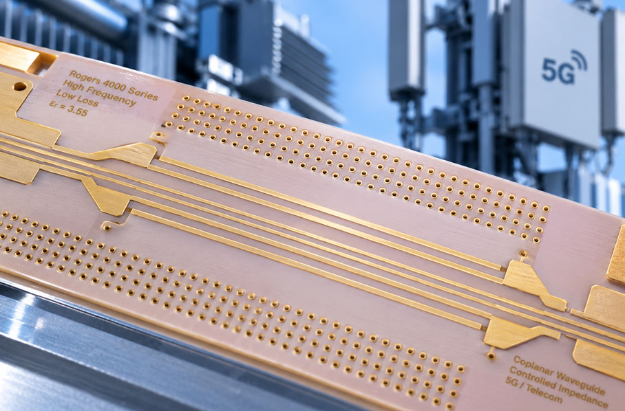
Telecom & 5G Infrastructure
Fabricated with ultra-low-loss Rogers laminates and precision-controlled impedance, delivering high-frequency bare boards that ensure signal integrity for 5G base stations and optical telecom networks.
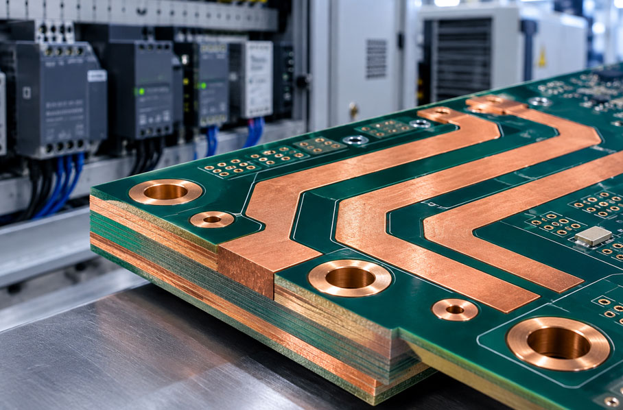
Industrial Automation & Control
Constructed with robust multilayer architectures and thick copper options to handle heavy electrical currents, thermal shock, and rigorous industrial environments.
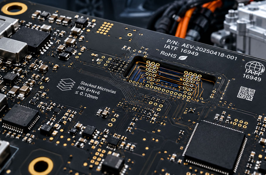
Automotive & EV Systems
Manufactured under strict IATF 16949 standards, providing zero-defect reliable bare PCBs designed to withstand harsh vibration and thermal stress in ADAS and EV powertrains.
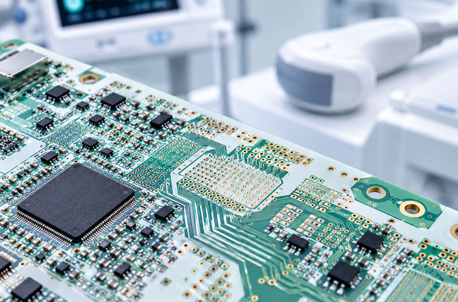
Medical Electronics & Diagnostics
Engineered to ISO 13485 standards with microscopic precision, delivering clean, highly dependable bare substrates for life-critical imaging and portable medical devices.
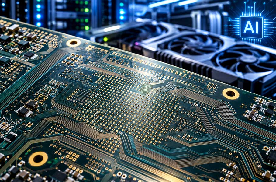
AI & High-Performance Computing
Utilizing Any-Layer HDI and ultra-fine line etching (down to 1.8 mil) to handle massive data throughput, high-speed signal routing, and thermal demands for AI accelerators.
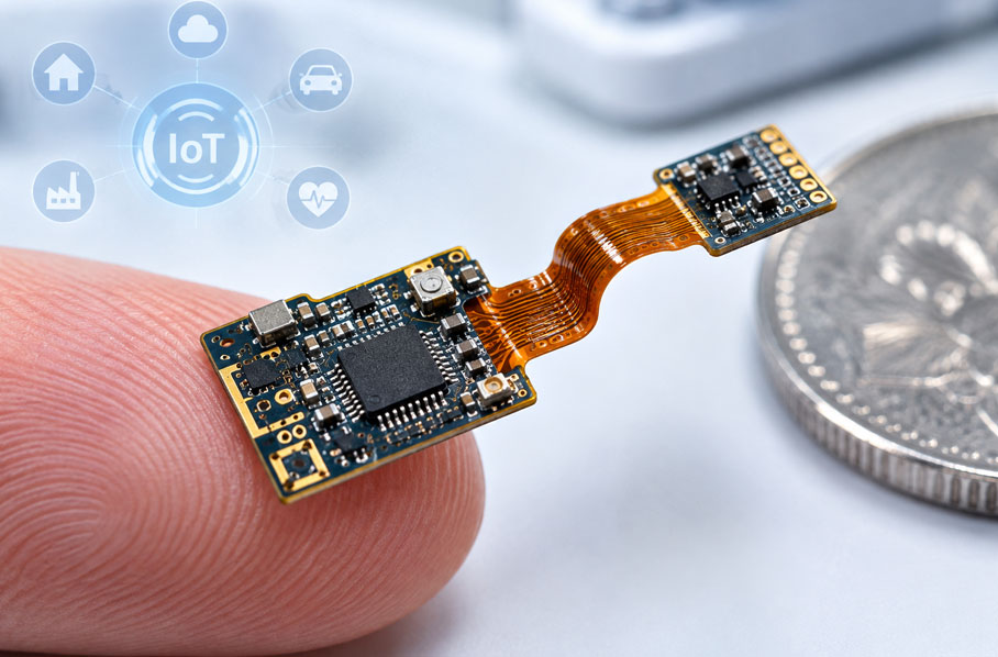
Smart IoT & Wireless Modules
Providing ultra-compact, high-density rigid and rigid-flex bare boards designed for spatial constraints, wearable tech, and smart wireless connectivity.
Custom PCB Manufacturing FAQs
Q1: What is the difference between PCB manufacturing and PCBA?
A: PCB manufacturing (fabrication) focuses on producing the physical bare board—including etching copper layers, drilling holes, and applying solder mask based on layout designs. PCBA (Assembly) involves mounting and soldering electronic components onto that fabricated bare board.
Q2: What is the maximum layer count and structure types you can fabricate?
A: We support rigid PCBs from 1 to 64 layers, alongside advanced flexible circuits (flex PCBs), rigid-flex boards, and complex Any-Layer HDI architectures.
Q3: What are your capabilities regarding fine-line etching and laser microvias?
A: We master ultra-fine line widths and spacings down to 1.8 mil (approx. 0.045 mm) and laser-drilled microvias down to 3 mil (approx. 0.075 mm) to support high-density routing.
Q4: How do you handle high-frequency materials for RF and microwave applications?
A: We utilize specialized low-loss laminates such as Rogers and Isola series, ensuring strict dielectric thickness control and minimal signal attenuation for high-frequency systems.
Q5: What surface finish options are available for bare PCBs?
A: We provide a full spectrum of surface finishes including ENIG, ENEPIG, Immersion Silver, lead-free HASL, and OSP to ensure long-term shelf life and superior soldering reliability.
Q6: What is your maximum copper weight capacity for heavy-current boards?
A: We support heavy copper fabrication up to 28 oz, making our bare boards ideal for high-power distribution, automotive EV systems, and industrial power supplies.
Q7: What quality control and testing methods are applied before delivery?
A: Every bare board undergoes 100% automated optical inspection (AOI), flying probe electrical testing, and rigorous impedance verification to ensure zero defects.
Q8: What drilling accuracy and aspect ratios can your smart factory achieve?
A: Our high-precision CNC and laser drills achieve positioning accuracy of up to ±1 mil (±0.025 mm) and support high-aspect-ratio plating up to 40:1 for multi-layer vertical interconnections.
Q9: Which international manufacturing and safety standards do you comply with?
A: Our production ecosystem complies with ISO 9001, ISO 14001, ISO 13485, IATF 16949, UL certifications, as well as strict RoHS and REACH environmental regulations.
Q10: What information or files are required to get a DFM review and quotation?
A: You need to provide standard Gerber files (RS-274-X format), an ODB++ package, a detailed drill file, and a fabrication drawing specifying layer stack-up, material preferences, and surface finish requirements.
Ready to Scale Your PCB Production? Contact Our Engineers Now.
Partner with KingTop Technology for reliable, high-precision PCB manufacturing solutions. Contact our engineering team today to discuss your bare board requirements.