The profound transformation of the automotive industry has positioned intelligent driving as a critical battleground where automakers compete for dominance. As the industry transitions from Level 2 (L2) driver assistance to advanced intelligent driving (Level 3 and above), the demands for computing throughput and data bandwidth within the perception, decision-making, and execution clusters have skyrocketed exponentially.
As the computational core of vehicle intelligence, the Automotive Domain Controller (ADC) bears the heavy load of complex tasks such as multi-sensor fusion, high-precision positioning, and real-time trajectory planning.
Within this hardware architecture, the PCB design and assembly (PCBA) processes—encompassing the core domain controller chips and peripheral circuitry—directly determine the system’s performance ceiling, energy efficiency, thermal management limits, and automotive-grade reliability throughout its entire lifecycle.
I. Intelligent Driving and Automotive Domain Controllers
Evolution and Classification of Intelligent Driving Systems
According to the standards set by the Society of Automotive Engineers (SAE), intelligent driving is categorized into six levels, ranging from L0 to L5. The market is currently in a transitional phase, moving from L2+ systems toward the large-scale commercial deployment of L3 and L4 technologies.
As systems evolve from single-function ADAS (such as AEB and LKA) to comprehensive, vehicle-wide intelligence, the number of sensors has increased dramatically—incorporating multiple high-resolution cameras, 4D millimeter-wave radars, LiDAR, and ultrasonic sensors. Consequently, data throughput has surged from hundreds of megabits per second in the past to tens or even hundreds of gigabits per second.
The Core Role and Architectural Evolution of Automotive Domain Controllers (ADCs)
Traditional automotive electrical/electronic (E/E) architectures relied on distributed Electronic Control Units (ECUs), where each function corresponded to a specific microcontroller. This approach resulted in redundant wiring harnesses, fragmented computing power, and difficulties in performing software upgrades.
Modern intelligent vehicles are rapidly shifting toward domain-centralized architectures and even “central computing plus zonal control” architectures. Automotive domain controllers integrate high-performance SoCs (such as NVIDIA Orin/Thor, Qualcomm SA8295P, and Huawei Ascend), microcontrollers (MCUs), high-capacity memory (LPDDR5/UFS), power management ICs (PMICs), and high-speed Ethernet switch chips. As the central hub of automotive computing, the domain controller is characterized by high computing power, high integration, high data bandwidth, and low power consumption; these attributes pose disruptive challenges to the underlying hardware platform.
Extreme challenges posed by intelligent driving to hardware (specifically PCBs and assembly)
Extreme operating environments: Automotive environments are harsh; PCBs must withstand intense mechanical vibration, wide temperature ranges (-40°C to 125°C or higher), high humidity, and chemical corrosion.
Ultra-high-speed signal integrity: The widespread adoption of high-speed interfaces—such as PCIe Gen4/Gen5, MIPI CSI-2, and 10G/100G automotive Ethernet—imposes stringent requirements regarding PCB impedance control, signal loss, and crosstalk suppression.
High heat flux dissipation: The concentrated heat generated by computing chips with power ratings in the hundreds of watts necessitates PCBs with efficient thermal conduction paths and thermal management designs.
Functional safety and reliability standards: Intelligent driving domain controllers typically must meet ASIL D (the highest Automotive Safety Integrity Level) standards; consequently, PCB design and assembly require exceptional fault tolerance and zero-defect manufacturing processes.
II. PCB Architecture and Design Specifications for Intelligent Driving Domain Controllers
Selection and characteristics of high-speed, high-frequency PCB materials
Dielectric constant (Dk) and dissipation factor (Df): To minimize attenuation and dispersion during high-speed signal transmission, automotive high-frequency/high-speed PCBs can no longer rely on traditional FR-4 materials. Instead, they widely utilize low-loss and ultra-low-loss high-frequency copper-clad laminates (CCL), such as Panasonic’s Megtron 6 and Megtron 7 or the Rogers series of materials.
Coefficient of Thermal Expansion (CTE) matching: The Z-axis CTE of automotive-grade PCB materials must closely match that of the copper foil and packaging substrate to prevent plated-through-hole (PTH) fracture or delamination during extreme temperature cycling.
CAF (Conductive Anodic Filament) resistance: Automotive PCBs must employ resin systems with excellent CAF resistance to prevent short-circuit failures caused by copper ion migration in high-humidity, high-voltage environments.
Stack-up Design and Impedance Control
Multilayer Board Structure Design: Advanced automotive domain controllers typically utilize multilayer board structures ranging from 16 to 24 layers or even higher densities. Stack-up planning adheres to the principle of placing signal layers immediately adjacent to reference planes, ensuring that every high-speed signal layer has a complete and continuous GND (ground) or PWR (power) plane as a reference.
Precise Impedance Control: For differential impedance (e.g., 85Ω or 100Ω) and single-ended impedance (e.g., 50Ω), PCB design engineers must strictly control impedance tolerance to within ±10% by precisely calculating dielectric thickness, copper thickness, and trace width/spacing.
Hybrid Lamination and Stepped Slot Technology: For domain controllers integrating RF and digital circuits, hybrid lamination (combining high-frequency materials with standard FR-4) is often employed to balance cost and high-frequency performance.
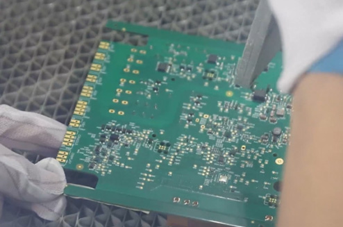
Power Integrity (PDN) and Signal Integrity (SI) Design
Power Distribution Network (PDN) Impedance Optimization: Computing SoCs generate massive transient currents; excessive PDN impedance can lead to voltage droop. Designs must minimize high-frequency impedance through the use of large-area power/ground planes, embedded capacitors, and decoupling capacitor networks placed in close proximity to chip pins.
High-Speed Bus Routing Specifications: For high-speed buses such as PCIe and DDR5, strict standards are enforced regarding trace length matching, serpentine routing, ground guard tracing, and prohibitions against crossing split planes to prevent electromagnetic crosstalk and signal reflections.
Thermal Design and Heat-Dissipating PCB Layout
Embedded Copper Blocks and Thermal Via Arrays: For high-heat core areas (such as SoCs), designs often incorporate embedded copper blocks or thick copper layers within the PCB, utilizing dense arrays of micro-thermal vias to rapidly conduct heat to the heat-dissipating baseplate at the bottom. Thermal Isolation: Physically isolate high-heat components—such as power management ICs (PMICs) and power devices—from temperature-sensitive analog front-end circuits and crystal oscillators to prevent heat-induced frequency drift or performance degradation.
Electromagnetic Compatibility (EMC) and Safety Design
Multi-level Grounding Strategy: Employ a hybrid grounding approach combining single-point and multi-point grounding. Segregate digital, analog, and power grounds, connecting them at critical boundaries via ferrite beads or 0-ohm resistors at a single point.
Shielding Cans and Edge Grounding: Design continuous shielding frame pads for critical RF and high-speed processing areas, and populate the PCB edges with dense shielding vias. This creates a “Faraday cage” effect, suppressing electromagnetic interference (EMI) and enhancing immunity to external interference (EMS).
III. PCB Assembly (PCBA) and Manufacturing Technology for Intelligent Driving Domain Controllers
High-Density Interconnect (HDI) and Advanced Packaging Substrate Technology
Any-layer HDI Technology: Due to the extremely high pin counts and fine pitches of SoC chips (e.g., BGA packages), traditional mechanical drilling can no longer meet routing density requirements. Automotive domain controllers widely utilize laser microvias, buried vias, and Any-layer HDI technology to achieve fine-channel interconnections between layers.
Package-level Adaptability: Modern intelligent driving chips often employ Flip Chip (FC-BGA) or System-in-Package (SiP) technologies, imposing stringent requirements on micro-solder joint flatness and flux residue control.
Rigorous Standards for Surface Mount Technology (SMT) in Automotive Electronics
IPC-A-610 Class 3 Standard: The manufacturing and acceptance of automotive-grade PCBA must strictly adhere to Class 3—the electronics industry’s highest reliability standard. This entails extremely strict criteria regarding component misalignment, solder paste volume/fullness, and solder joint wetting angles.
Placement Accuracy for Miniature Components: With the widespread use of passive components as small as 01005 (or even smaller) and fine-pitch QFN/BGA packages, high-speed, high-precision SMT placement machines must feature vision alignment and constant-temperature control to ensure placement offsets are kept within the micrometer range.
Soldering Process and Reliability Control
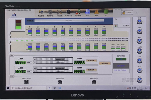
Vacuum Reflow Soldering: To completely eliminate internal voids in large power chips and BGA solder joints, vacuum reflow soldering technology is widely adopted in the manufacturing of automotive domain controllers. By strictly controlling the soldering void ratio to below 5% (or even lower), thermal conductivity and fatigue resistance are significantly improved.
Lead-Free Eutectic Alloy Selection: SAC305 (Tin-Silver-Copper) lead-free solder is typically used; temperature profile optimization is employed to prevent component micro-cracks caused by thermal stress.
Conformal Coating and Dispensing/Potting Processes
Conformal Coating: To withstand moisture, condensation, salt spray, and sulfur corrosion in automotive environments, PCBA assemblies must undergo precision conformal coating (using materials such as acrylic, polyurethane, or silicone resin). Selective coating machines are used to precisely avoid areas such as connector sockets and heat-dissipation contact surfaces.
Underfill and Edge Bonding: For BGA packages and heavy components, capillary underfill or adhesive reinforcement (dispensing) is applied, greatly enhancing the solder joints’ resistance to mechanical vibration and thermal cycling shock.
IV. Testing, Verification, and Quality Control for Smart Driving Automotive Domain Controller PCBs
Design for Manufacturability (DFM) and Design for Testability (DFT)
DFM Simulation: DFM (Design for Manufacturing) and DFA (Design for Assembly) simulation analyses are conducted during the PCB design phase to identify structural risks—such as cold solder joints, bridging, or stress concentration—at an early stage.
DFT Layout: Test points and boundary scan (JTAG) chains are strategically reserved on the circuit board to ensure efficient electrical performance testing during mass production.
Advanced Production Line Testing Technologies
SPI (Solder Paste Inspection) & AOI (Automated Optical Inspection): Real-time 3D SPI and multi-angle AOI are performed during the printing and SMT (Surface Mount Technology) stages to intercept early-stage defects such as insufficient solder paste, misalignment, and incorrect component placement.
3D X-ray Inspection (AXI): Used for radiographic inspection of hidden BGA solder joints, internal vias in multilayer boards, and the soldering quality and voiding status of embedded components.
ICT (In-Circuit Testing) & FCT (Functional Testing): Comprehensive automated scanning of the entire board—covering electrical connections, component parameters, and the integrated hardware-software functionality of autonomous driving domain controllers—is conducted using bed-of-nails fixtures or dedicated test jigs.
Automotive-Grade Environmental and Reliability Verification
Thermal Cycling: Thousands of cycles are performed in a temperature chamber ranging from -40°C to 125°C to test the thermal fatigue resistance and lifespan of solder joints and board materials.
Vibration & Mechanical Shock Testing: Simulates the full-frequency vibration spectrum experienced by vehicles on rough roads to verify the mechanical strength of PCB structural components and heavy-duty connectors.
HALT/HASS (Highly Accelerated Life Testing / Highly Accelerated Stress Screening): Stresses exceeding design limits are applied to rapidly expose latent design and process defects, ensuring a zero-failure rate over the product’s design lifespan (typically 10–15 years).
V. Future Trends and Technological Outlook
Evolution of Centralized E/E Architectures and Central Computing Platforms
Future automotive E/E (Electrical/Electronic) architectures will evolve further toward a “central computing + zonal controller” model. In-vehicle domain controllers will shift from “independent domains” (e.g., autonomous driving, cockpit, and vehicle control domains) to “cross-domain integration” (e.g., cockpit-driving integration and vehicle-wide central computing).
This transformation requires PCB designs to support higher-density optoelectronic hybrid transmission, higher-layer-count HDI (High-Density Interconnect) boards, and more complex power distribution networks.
New Requirements for PCB Manufacturing Driven by Modular and Standardized Design
To reduce R&D costs and shorten time-to-market, automakers and Tier 1 suppliers are vigorously promoting modular computing designs (such as standardized core computing modules for autonomous driving). This has driven the rapid evolution of PCB design toward standardized interfaces, high-density board-to-board connectors, and modular thermal management designs.
Green Manufacturing and the Use of Low-Carbon, Eco-friendly Materials
Driven by global “dual-carbon” goals, the manufacturing of automotive PCBs is increasingly adopting halogen-free materials, recyclable eco-friendly resins, and low-carbon production processes.
Simultaneously, the use of digital twin technology and AI-assisted design tools allows for the optimization of PCB routing and thermal dissipation paths, achieving an ideal balance between manufacturing energy consumption and performance.
Conclusion
The design and assembly of PCBs for intelligent driving domain controllers constitute a highly complex, interdisciplinary, and multidimensional system engineering task. Success requires not only deep expertise in high-speed circuit design and thermal management but also relies on sophisticated automotive-grade manufacturing processes and rigorous quality control systems.
As advanced intelligent driving becomes increasingly widespread, continuous breakthroughs in PCB hardware and software technologies will provide a solid hardware foundation for the evolution of automotive intelligence.