When building a high-performance AI robot, PCB (Printed Circuit Board) design and assembly are critical factors determining motion precision, sensing stability, and system robustness.
Because AI robots integrate high-performance edge computing chips, precision drive systems, extensive sensor arrays, and complex power management networks, their PCB design must balance high-density routing, robust electromagnetic compatibility (EMC), excellent thermal management, and strict mechanical constraints.
Driven by the rapid advancement of edge computing and AIGC technologies, the hardware architecture of modern AI robots is evolving toward high integration, heterogeneous computing, and high dynamic response. The following is a comprehensive guide to PCB design and assembly tailored specifically for AI robots.
I. Architectural Planning and Component Selection for AI Robot PCB Systems
Before drafting schematics, a systematic top-level design of the robot’s overall electrical architecture is essential. AI robots typically employ either a heterogeneous distributed architecture or a highly integrated single-board design; sound planning serves as the foundation for ensuring subsequent signal integrity and system stability.
Design Specifications for Main Control and Computing Units
Heterogeneous Computing Division of Labor: A common architecture combines an “edge AI computing core” (e.g., NVIDIA Jetson series, Raspberry Pi Compute Module) with a “real-time motion control MCU” (e.g., STM32H7, ESP32-S3). High-performance chips handle tasks such as visual SLAM, deep learning inference, and navigation algorithms, while real-time MCUs manage low-level motor PID control, sensor data acquisition, and safety emergency stops.
Separation of Core Module and Carrier Board: A “Core Module + Carrier Board” design is recommended. The core module handles complex routing for the CPU/GPU and high-speed memory (LPDDR), while the carrier board focuses on peripheral interface expansion, power distribution, and power driving; this approach effectively reduces design risk and facilitates future iterations.
System Boot and Storage: High-speed interfaces—such as eMMC, NVMe SSD, and MicroSD—require routing that strictly adheres to the chip manufacturer’s recommended topology to minimize trace length mismatch. 2. Power Management and Power Supply Topology
Multi-rail power requirements: AI robots involve various voltage levels. The main control chip typically requires multiple power rails—such as 5V, 3.3V, 1.8V, 1.1V, and 0.8V—for core and I/O operations; sensors require 5V or 12V; and motor drivers require high voltages of 12V, 24V, or even 48V.
Isolation between power and logic: Physical or electrical isolation between motor power and logic power is essential. Starting or stopping high-power motors generates severe voltage transients (surges and back-EMF); sharing a power source could cause main controller resets or ADC sampling distortion.
Power efficiency and ripple control: High-efficiency switching regulators (Buck DC-DC converters) are used for high-current step-down conversion, while Low-Dropout Regulators (LDOs) must be placed ahead of sensitive analog circuits (such as IMUs, audio components, and ADC reference sources) to filter out high-frequency noise.
Sensor and Communication Bus Interface Planning
High-speed buses: Camera modules (MIPI CSI-2), depth cameras (USB 3.0/GigE), and LiDAR (Ethernet/UART) have extremely high requirements for bandwidth and interference immunity, necessitating designated PCB areas for differential pair impedance control.
Control buses: Chassis and joint motors commonly utilize CAN bus or RS485 serial bus interfaces. CAN bus routing requires attention to 120Ω terminal matching resistors and a daisy-chain topology.
II. AI Robot PCB Schematic Design and High-Frequency/High-Speed Design Considerations
The schematic is not merely a logical representation of connections; it serves as the first line of defense for hardware reliability. Rigorous design eliminates electrical hazards at the source.
Schematic Design Guidelines and Safety Protection
ESD and Surge Protection: TVS diodes (Transient Voltage Suppressors) and common-mode chokes must be placed near all exposed interfaces (USB, Ethernet, CAN, serial ports, external sensor sockets).
Power Supply Reverse Polarity and Overcurrent Protection: The main power input stage should incorporate a P-MOSFET reverse-polarity protection circuit and a series-connected resettable fuse (Polyfuse) or electronic fuse (eFuse).
Emergency Stop Chain Design: Safety-critical mobile robots must feature a hardware-level Emergency Stop circuit at the schematic level, capable of directly cutting off the motor driver enable signal or the main power contactor.
High-Speed Signal and Bus Impedance Matching
Single-ended and Differential Impedance Control:
Single-ended traces (e.g., standard GPIO, control signals): Typically controlled at 50 Ω.
High-speed differential pairs (e.g., MIPI CSI, USB 2.0/3.0, Ethernet): Impedance strictly controlled at 100 Ω (differential).
Crosstalk Suppression and Guard Tracing: Clock lines, high-frequency crystal oscillators, and high-speed buses require guard traces (ground traces) on both sides, accompanied by stitching vias, to minimize crosstalk with surrounding sensitive circuits.
Mixed-Signal Isolation and Interference Immunity (EMC/EMI)
Ground Plane Partitioning and Single-Point Connection: Digital ground (DGND), analog ground (AGND), and power ground (PGND) must be carefully planned during layout and ultimately tied together at a single point—typically near the power input or ADC chip—to prevent high-current ground noise from contaminating the reference ground for small signals.
Decoupling Capacitor Configuration: Decoupling capacitors must be placed close to the power pins of every IC (typically a 0.1 μF ceramic capacitor in parallel with a 10 μF tantalum or high-capacity ceramic capacitor); high-frequency decoupling capacitors should be positioned as close as possible to the chip’s VDD pin.
III. Practical Strategies for PCB Layout and Thermal Design
A sound physical layout is crucial to PCB performance, particularly for AI robots characterized by space constraints and significant heat generation.
Stack-up Design and Lamination Planning
For complex AI robot motherboards, a 4-layer or 6-layer PCB structure is recommended:
Recommended stack-up for a typical 6-layer board:
Top Layer: Signal layer, high-speed traces, and key components.
Layer 2 (Internal Plane 1): Solid ground plane (GND) to provide a low-impedance return path.
Layer 3 (Internal Plane 2): Signal layer or auxiliary power layer.
Layer 4 (Internal Plane 3): Main power plane (e.g., 5V, 3.3V).
Layer 5 (Internal Plane 4): Solid ground plane (GND) to enhance shielding.
Bottom Layer: Signal layer and surface-mount (SMD) passive components (resistors/capacitors).
Physical Isolation of Power and Logic Zones
Zoning principle: Divide the PCB into “High-Voltage/Power Zone,” “Digital Computing Zone,” and “Analog/Sensor Zone.”
High/Low-Voltage Isolation: Motor driver chips, high-power MOSFETs, and relays should be grouped at the PCB edge or in a separate area, away from the main CPU and highly sensitive inertial sensors (IMU), to prevent electromagnetic radiation from causing sensor drift.
Thermal Design and High-Power Component Placement
Heat Dissipation: The AI computing core (e.g., Jetson module), Power Management IC (PMIC), and motor driver chips are the three primary heat sources.
Thermal Via Arrays: Place dense arrays of thermal vias (0.3mm–0.5mm diameter) beneath or around the pads of heat-generating components to rapidly conduct heat to copper dissipation planes on internal or bottom layers.
Provision for Heatsinks and Fans: Ensure sufficient physical space during layout for the installation of aluminum heatsink fins, thermal pads, or cooling fans.
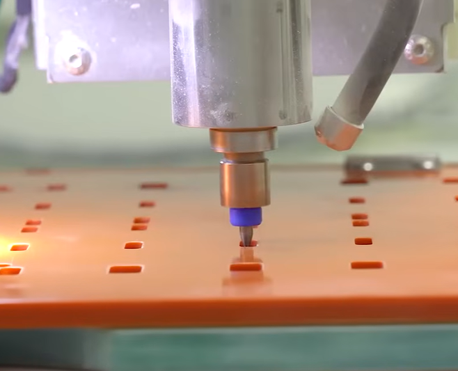
IV. Process Guidelines for Assembly, Soldering, and Hardware Debugging
Once the design is complete and Gerber files have been submitted to the PCB manufacturer, the project enters the critical assembly and soldering phase.
Component Selection and SMT Stencil Design
Component Selection: Prioritize industrial-grade components (rated for -40°C to +85°C or higher)—particularly electrolytic capacitors, connectors, and power inductors—as the vibrations encountered during robot operation place high demands on mechanical robustness.
Stencil Thickness and Aperture Design: For fine-pitch QFNs, BGAs, and chips with fine leads, a 0.12mm thick laser-cut stainless steel stencil is recommended. Stencil apertures should be slightly enlarged relative to component pad sizes or designed with anti-solder-bead features (such as grid-pattern apertures).
Reflow Soldering Profiles and Manual Soldering Precautions
SMT Reflow Soldering Process:
Establish a scientifically sound temperature profile: Preheat, Soak, Reflow, and Cooling stages. The peak temperature is typically set 20°C–25°C above the melting point of lead-free solder paste (SAC305), resulting in a range of approximately 245°C–250°C.
Manual Soldering and Rework Standards:
When soldering components with large thermal pads, use a temperature-controlled soldering iron in conjunction with a preheating station to prevent cold solder joints.
After soldering, thoroughly remove flux residue using anhydrous ethanol or a specialized cleaning agent to prevent leakage currents or corrosion during long-term operation.
Integrated Hardware-Software Debugging and Troubleshooting
Smoke Test: Strictly avoid connecting the board directly to the full-voltage power supply during the initial power-up. Instead, use a digital adjustable DC power supply with current-limiting capabilities; set a low current limit (e.g., 500mA) and monitor the quiescent current to ensure it is within normal limits.
Step-by-step power rail verification: Use a digital multimeter and oscilloscope to measure each voltage output (5V, 3.3V, 1.8V) for accuracy and ensure ripple levels remain within permissible limits.
Communication and peripheral integration testing:
Flash low-level firmware via the SWD/JTAG interface and test serial port (UART) output.
Capture bus waveforms using a CAN analyzer or oscilloscope to verify seamless communication protocol operation across modules.
Gradually initialize the AI computing core, run basic perception and motion control nodes, and conduct real-world field testing and dynamic tuning of the complete system.
Expert Tip: AI robot PCB hardware development is an iterative optimization process. During the initial prototyping phase, it is advisable to incorporate ample test points and 0-ohm resistor jumpers. This ensures flexibility for hardware modifications—such as trace cutting, “flying wire” rework, or parameter adjustments—should signal integrity issues or circuit defects arise later.
Conclusion
KingTop Technology Empowers AI Robot Hardware
Building high-performance AI robots requires not only advanced algorithms but also a stable, reliable, and highly integrated hardware foundation. From complex heterogeneous computing architecture planning and rigorous high-speed signal/anti-interference design to precise zonal layout and thermal management, every stage profoundly impacts the robot’s ultimate performance and service life.
As an industry-leading provider of electronics manufacturing and circuit board solutions, KingTop Technology specializes in serving global clients with services ranging from high-precision PCB fabrication, SMT (Surface Mount Technology), and DIP (Dual In-line Package) assembly to comprehensive PCBA assembly and testing.
To meet the rigorous demands of AI robots—including high-layer-count boards, High-Density Interconnect (HDI) technology, high-power thermal management, and resistance to shock and interference—KingTop Technology leverages mature industrial-grade process standards, strict quality control systems, and efficient capabilities for transitioning from prototype to mass production. We build a robust hardware foundation to help your AI robot products reach the market quickly!