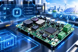
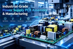
This high-performance PCB assembly design solution for AI integrates advanced computing and intelligent manufacturing, fully overcoming the limits of high-speed signal integrity and thermal management to achieve a comprehensive leap toward digital and intelligent end-to-end capabilities.
Driven by the demands of hyperscale data centers, intelligent connected vehicles, aerospace telemetry and control systems, and high-end medical imaging equipment, circuit board operating frequencies have generally entered the millimeter-wave and high-speed serial link era. Consequently, signal transmission loss, electromagnetic interference, and localized heat flux density are rising exponentially.
Traditional design and assembly models—reliant on manual experience and static, rule-based approaches—suffer from long development cycles and high trial-and-error costs. Moreover, they struggle to achieve globally optimal solutions amidst complex spatial constraints and multi-physics coupling effects.
Against this backdrop, AIGC technology—which deeply integrates advanced computational models with automated manufacturing—is reshaping the entire high-performance PCB assembly design process. By employing algorithms for multi-dimensional collaborative optimization and closed-loop simulation of massive design parameters, this technology fundamentally breaks through the bottlenecks of traditional processes, enabling a comprehensive intelligent leap from design through to manufacturing.
I. Core Pain Points and Evolving Requirements in AI-Driven High-Performance PCB Assembly Design
Challenges of High-Speed Signal Integrity and Fine-Pitch Layout
In current designs involving multi-layer High-Density Interconnect (HDI) and ultra-high-frequency boards, signal transmission rates have surpassed tens of Gbps. As trace density increases sharply, factors such as characteristic impedance continuity (for microstrip and stripline), the skin effect, dielectric loss, and crosstalk between fine-pitch components become extremely critical.
Traditional design tools often rely on post-design simulation or an engineer’s intuition, frequently struggling to balance competing priorities when managing thousands of network nodes. The widespread adoption of fine-pitch components (such as CSP and BGA packages with pitches of 0.3mm or less) imposes rigorous demands on pad design, solder mask dam width, and escape routing.
Even minute layout deviations can lead to signal reflections, eye diagram closure, or excessive timing jitter. Consequently, employing intelligent methods to plan topological constraints for high-frequency-sensitive areas during the initial layout phase has become a fundamental prerequisite for ensuring the stable operation of high-performance circuits.
2. Precision Control of Thermal Management and Stress Distribution in Complex Multilayer Boards
The power density of high-performance electronic systems is experiencing explosive growth—particularly in high-power computing acceleration cards, automotive domain controllers, and power modules—where localized heat flux often exceeds tens or even hundreds of watts per square centimeter.
Uneven heat accumulation not only causes component operating temperatures to exceed safe thresholds but also generates immense thermomechanical stress due to differences in the coefficients of thermal expansion (CTE) among various materials during reflow soldering and subsequent thermal cycling.
Such stress frequently leads to fatigue cracking in solder joints, tearing of copper foil, or substrate delamination. A major technical challenge facing engineers today is how to jointly optimize heat sinks, thermal via arrays, and power component layouts in three-dimensional space, while precisely controlling temperature profiles during the assembly process.
Limitations of Traditional Processes in High-Mix, Low-Volume Flexible Manufacturing
As the lifecycles of electronic products shorten, the “High-Mix, Low-Volume” production model has become the norm.
On traditional production lines, switching between product batches requires engineers to spend significant time optimizing stencils, fine-tuning pick-and-place machine programs, reconfiguring reflow oven temperature profiles, and setting parameters for AOI (Automated Optical Inspection) and AXI (Automated X-ray Inspection).
Such frequent manual intervention is not only inefficient but also prone to human error, resulting in inconsistent first-article pass rates and lengthy line-changeover times.
Developing an intelligent assembly system capable of adaptive adjustment and self-learning—enabling the switching of process parameters in seconds and dynamic compensation—is essential to meeting the demands of modern flexible manufacturing for high quality and short delivery times.
II. AIGC-Based Architecture Design for Intelligent PCB Layout and Routing
Deep Learning-Driven Optimization Model for Automated Component Placement
Component placement is the primary stage of modern PCB design; it directly determines electrical performance, heat dissipation paths, and the feasibility of subsequent assembly. The intelligent placement model, based on deep reinforcement learning, treats the PCB surface as a high-dimensional coordinate grid and converts the netlist connections from the schematic into nodes and edges within a Graph Neural Network (GNN).
- Multi-objective collaborative optimization: During training, the model simultaneously considers minimizing total bus length, ensuring direct high-speed signal paths, evenly distributing high-heat components, and physically isolating sensitive analog circuits from digital switching power supplies.
- Spatial constraint alignment: The algorithm automatically identifies and adheres to rigid geometric constraints—such as mounting holes for structural components, edge connectors, and enclosure height limits—thereby eliminating the inefficient, repetitive manual layout adjustments typical of traditional workflows.
- Accelerated layout convergence: By incorporating attention mechanisms, the model rapidly focuses on critical high-speed link groups, reducing the time required for iterative manual layout from days to minutes while significantly improving electrical performance metrics.
Algorithmic fusion of intelligent routing and impedance control
The routing phase is critical to the success of a PCB. AIGC technology combines traditional numerical electromagnetic field solvers with machine learning surrogate models to enable real-time impedance calculation and path planning for complex multi-layer board routing.
- Dynamic impedance prediction: As traces are extended, the algorithm calculates instantaneous impedance in real-time based on surrounding reference planes, dielectric thickness, and copper thickness, automatically correcting the path before design rule check (DRC) violations occur.
- Serpentine routing and length-matching optimization: For timing-critical DDR buses or differential pairs, the intelligent routing engine automatically generates smooth routing paths based on crosstalk minimization principles, effectively suppressing electromagnetic interference (EMI).
- Via matrix optimization: Through intelligent planning that combines blind vias, buried vias, and back-drilling processes, the negative impact of via parasitic capacitance and inductance on high-speed signal integrity is minimized.
Proactive prediction and avoidance of signal crosstalk and electromagnetic compatibility (EMC) issues
At the design inception stage, the AIGC engine utilizes Generative Adversarial Networks (GANs) to perform virtual simulations of the electromagnetic field distribution across the entire PCB.
- Early Identification of Hotspots: Before physical board fabrication, the system can precisely pinpoint potential crosstalk hotspots, areas with discontinuous return paths, and frequency bands prone to excessive radiation.
- Automatic Shielding and Ground Via Fences: For highly sensitive areas, the algorithm automatically recommends and generates ground via arrays (guard traces/ground via fences) to establish robust electromagnetic shielding barriers, thereby significantly enhancing the system’s anti-interference capabilities at the fundamental design level.
III. Optimization Solutions for High-Density Assembly and Microelectronic Manufacturing Processes
High-Precision Alignment and Solder Quality Control in Surface Mount Technology (SMT)
When a design transitions to physical assembly, precision control on the SMT production line becomes critical. Traditional machine vision alignment faces extreme challenges when dealing with miniature chip components, 01005 packages, and ultra-fine-pitch QFN and BGA components.
- Sub-micron Machine Vision Compensation: By integrating high-resolution multispectral imaging and deep-learning-based edge extraction algorithms, the system can identify minute deformations and thermal expansion/contraction shifts in PCB fiducial marks in real-time, dynamically adjusting the placement head coordinates.
- Adaptive Adjustment of Printing Parameters: Solder paste printers utilize AI algorithms to perform real-time, closed-loop adjustments of squeegee pressure, print speed, and separation speed. These adjustments are based on ambient temperature and humidity, changes in solder paste viscosity, and the cleanliness status of the stencil from the previous cycle, ensuring consistent solder paste volume across boards.
Ensuring Soldering Reliability for Odd-Form Components and Micro-BGA Packages
High-performance boards often integrate a large number of high-density BGAs, PoP (Package-on-Package) stacked chips, and various heavy, odd-form connectors.
- Suppression of Solder Joint Voiding: Through intelligent control of air pressure in the reflow oven’s peak temperature and soak zones, internal solder bubbles are effectively expelled, keeping the voiding rate of BGA solder joints strictly within industry-leading standards.
- Flexible Gripping of Irregular Components: For high-performance connectors featuring non-standard dimensions and irregular geometries, a flexible gripper combined with force-feedback sensors is employed. AI algorithms adjust the downward pressing depth based on real-time impedance and pressure feedback, preventing localized overload or damage to the substrate.
Adaptive Intelligent Adjustment of Dynamic Hot-Air Reflow Profiles
The reflow oven temperature profile is the critical factor determining soldering quality. Subtle variations in copper foil thickness, thermal capacity, and component distribution across different PCB batches mean that fixed temperature profiles often fail to achieve optimal results across the board.
- Online Temperature Profile Identification: Infrared thermal imaging matrices are deployed at the reflow oven entrance and key heating zones. By integrating the board’s 3D CAD model with thermal capacity distribution data, the AI system calculates and predicts the actual heat absorption rate of the current board in each zone in real time.
- Dynamic PID Parameter Correction: The system automatically fine-tunes heating power and fan speeds in each zone to achieve dynamic closed-loop temperature control. This ensures that lead-free solder (such as SAC305) achieves adequate wetting during the preheat, soak, reflow, and cooling stages without causing thermal overload or micro-cracking in components.
IV. AI-Driven Online Quality Inspection and Closed-Loop Defect Control
Application of Machine Vision and Deep Learning in AOI/AXI
Traditional Automated Optical Inspection (AOI) and X-ray Inspection (AXI) systems often suffer from high false-call rates (“over-kill”), necessitating extensive manual secondary verification.
- Few-Shot Learning and Anomaly Detection: Leveraging deep convolutional neural networks, the model learns feature maps from vast datasets of defect-free units and various minute defects (such as micro-cracks, cold joints, bridging, and misalignment), achieving an exceptionally high defect detection rate (aiming for “Zero Defects”).
- 3D Topography Reconstruction and Volumetric Measurement: Utilizing multi-angle structured light scanning and AI-based 3D reconstruction technology, the system precisely measures solder joint height, volume, and wetting angles. This overcomes the limitations of traditional 2D AOI, which cannot inspect hidden solder joints (such as those beneath LGA or BGA components).
Real-time Welding Defect Recognition and Automated Production Line Parameter Adjustment
Quality inspection serves not merely as a “gatekeeper” but as a feedback source for continuous quality improvement.
- Root Cause Traceability: When AOI/AXI systems repeatedly detect a specific type of defect (e.g., cold solder joints at the edge of a BGA in a particular zone), AI algorithms automatically trace back to upstream parameters—such as squeegee pressure during the printing stage or component placement offset data.
- Closed-loop Process Correction: The system generates corrective instructions and automatically transmits them to upstream mounters or printers, enabling millisecond-level closed-loop control from detection to correction, thereby preventing batch defects at the source.
Full Lifecycle Quality Traceability and Big Data Analytics Platform
High-performance assembly solutions require robust traceability systems to meet the rigorous audit standards of high-end applications.
- Barcode/Laser Marking Enablement: Each PCB is assigned a unique laser-etched QR code at the start of the line, serving as its digital identity credential.
- Comprehensive Data Cloud Integration and Profiling: Data—including temperature profiles, pressure readings, visual inspection images, and component batch numbers—is written to a distributed database in real-time. Big data analytics models continuously generate yield prediction reports and equipment health assessments (predictive maintenance), providing a solid foundation for the factory’s digital transformation.
V. Intelligent Supply Chain and Flexible Production Scheduling
Intelligent Component Attribute Matching and Material Kitting Alerts
High-performance PCB assembly involves hundreds of types of precision components; material interchangeability and lifecycle management directly impact project delivery.
- Intelligent Material Attribute Comparison: The system automatically parses BOMs and schematics, utilizing natural language processing and vector retrieval technologies to accurately identify electrical parameters, package types, and lists of candidate substitute components.
- Intelligent Kitting Prediction: By integrating production schedules with supplier lead times, AI models provide dynamic alerts regarding material kitting status, effectively preventing line stoppages caused by the absence of even a single tiny resistor.
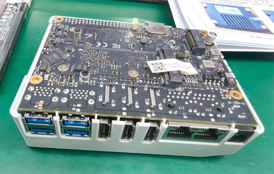
Dynamic Optimization of Production Scheduling and Equipment Load via Reinforcement Learning
In mixed-line production environments characterized by high product variety and small batch sizes, disruptions such as rush orders, equipment breakdowns, and material delays are commonplace, rendering traditional static schedules ineffective.
- Multi-constraint Reinforcement Learning Scheduling: Aiming to minimize changeover times, maximize equipment utilization, and meet the most urgent delivery deadlines, the reinforcement learning scheduling model can generate optimal dynamic schedules—comprising hundreds of process steps—within a single second.
- Adaptive Balancing of Bottleneck Processes: In the event of a sudden breakdown in a surface-mount technology (SMT) placement machine, the system automatically reassigns subsequent tasks to standby equipment of the same type and dynamically adjusts the production cadence of surrounding equipment, ensuring stable overall workshop throughput.
Intelligent Practices for Green, Low-Carbon Operations and Granular Energy Management
With the global emphasis on carbon emissions and sustainable development, optimizing energy consumption during manufacturing has become a crucial component of high-performance design solutions.
- Dynamic Equipment Energy Efficiency Management: Reflow ovens, placement machines, and large-scale HVAC/purification systems are integrated into an IoT monitoring network; AI algorithms automatically switch idle equipment to sleep or low-power modes based on real-time workshop production loads.
- Precise Carbon Footprint Accounting: By collecting real-time data on electricity, gas, and raw material consumption and applying carbon modeling conversions, the system generates comprehensive carbon footprint reports for each batch of high-end PCB assemblies, helping enterprises secure a leading position in the era of green, intelligent manufacturing.
Conclusion
The AI-driven high-performance PCB assembly design solution fundamentally transcends the physical limitations of traditional electronics manufacturing. Through the synergistic optimization of multi-physics fields, intelligent precision assembly, and end-to-end closed-loop quality control, it achieves a significant leap in efficiency from design to production.
This not only effectively resolves signal integrity and thermal management challenges associated with high-speed, high-density designs but also empowers enterprises to comprehensively improve yields and shorten production cycles amidst the wave of flexible, intelligent manufacturing, leading the industry into a new stage of high-quality development.