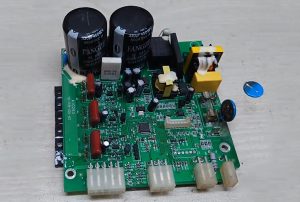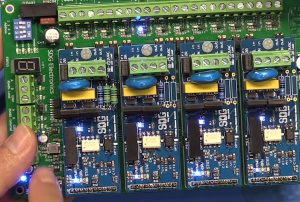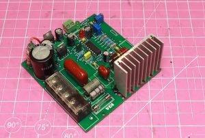

Serving as the “energy heart” of modern high-density, high-efficiency electronic systems, the Smart Power Management Module (SPMM) integrates multiple core functions, including power conversion, dynamic monitoring, fault diagnosis, and communication feedback.
Driven by the explosive growth of data centers, new energy vehicles, industrial automation, and advanced IoT devices, power modules are rapidly evolving toward higher power density, higher operating frequencies, and greater intelligence.
The manufacturing quality and efficiency of SPMMs depend not only on the selection of chips and components but also heavily on the precise control of PCB assembly (PCBA) processes and systematic engineering management.
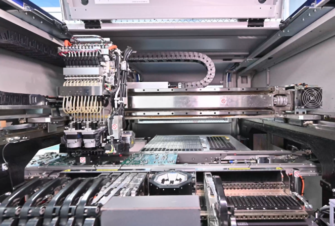
Because these modules typically feature the coexistence of high-current paths and low-voltage control signals, high heat flux density, significant high-frequency switching interference, and complex multi-chip packaging, their SMT (Surface Mount Technology) and DIP (Dual In-line Package/Through-Hole Technology) assembly processes face rigorous technical challenges.
I. Technical Evolution and PCB Design Characteristics of SPMMs
SPMMs typically achieve a high level of integration—combining power semiconductors (such as GaN MOSFETs, SiC MOSFETs, and IGBTs), main control microcontrollers (MCU/DSP/digital PWM controllers), high-precision sampling circuits (for current, voltage, and temperature), and isolated communication interfaces—within a compact PCB footprint. The module’s specific PCB design and structural characteristics directly dictate the technical approach for subsequent assembly processes.
Application of Hybrid Stack-ups and High-Thermal-Conductivity Substrates
Due to the extremely high heat flux density inherent in SPMMs, the choice of PCB substrate has moved beyond traditional standard FR-4 materials.
High-thermal-conductivity aluminum/copper substrates (IMS): Commonly used for mounting power devices on a single side, these substrates typically require thermal conductivity ratings ranging from 2.0 W/m·K to over 8.0 W/m·K and utilize thick copper foil (3 oz–6 oz) to handle high currents in the range of hundreds of amperes.
High-Tg Heavy Copper PCB: Utilizes modified FR-4 or halogen-free materials with a Tg > 170°C, combined with 2oz–4oz thick copper on inner layers, to achieve mixed-layer lamination of low-voltage control signal layers and high-current power layers.
Embedded Copper Coin Technology: Pure copper blocks are embedded directly beneath high-heat components (such as main power transistors and high-frequency inductors) to conduct heat to external heat sinks via a direct metal thermal path.
Mixed Layout Protocols for Low-Voltage Control and High-Voltage Power
The PCB layout of intelligent power management modules typically features a “partitioned high- and low-voltage” design:
Power Loop: Requires extremely short and wide traces to minimize parasitic inductance and I²R conduction losses.
Control and Sensing Loops: Traces for voltage sampling, current sensing (e.g., Kelvin connections), and PWM drive signals are fine and compact; being highly sensitive to noise, they must be routed away from nodes with high dv/dt and di/dt.
Thermal Isolation and Electrical Clearance: Must comply with safety standards such as IEC/UL 62368, maintaining strict creepage distances and electrical clearances between high-voltage and low-voltage sides, with extremely high cleanliness requirements for the isolation zones during assembly.
II. Comprehensive Analysis of Core PCBA Assembly Processes for Intelligent Power Management Modules
Given the characteristics of intelligent power management modules—high density, high thermal mass, and mixed high/low-voltage circuitry—PCBA assembly must rely on a foundation of high automation and precise process control.
Solder Paste Printing Process
Solder paste printing is a critical step that determines the First Pass Yield (FPY) of SMT assembly. In intelligent power management modules, components with ultra-small footprints (such as 0201/01005 chip resistors/capacitors and WLCSP control ICs) often coexist on the same board as high-thermal-mass power devices (such as D2PAK, TO-263, and PDFN packages). This presents significant challenges for controlling solder paste volume.
1. Step Stencil Design and Application
Given the coexistence of large power pads and fine-pitch ICs, a uniform-thickness stencil cannot simultaneously meet the requirements for paste release and volume control.
Step-down: In areas containing 0.4mm-pitch QFN/BGA components or 0201 devices, the stencil thickness is locally reduced from the standard 0.13mm to 0.10mm to prevent solder bridging.
Step-up: In areas with high-current connectors, high-power surface-mount inductors, or large MOSFETs, the thickness is increased to 0.15mm–0.18mm to ensure sufficient solder volume and mechanical strength for the solder joints.
2. Stencil Aperture Design: Strategies for Preventing Solder Balls and Voids
Window Pane Apertures: For power chips or MOSFETs featuring large exposed thermal pads on the bottom, the aperture design must utilize a “window pane” (grid) pattern. The area ratio is controlled between 50% and 70% to allow gas to escape during soldering—preventing large voids—and to avoid component floating, which could lead to open circuits (poor wetting) on peripheral pins.
Anti-Solder Balling Apertures: For chip power capacitors (size 0603 and larger), “U-shaped” or concave apertures are employed to minimize the risk of solder beads being squeezed out during the reflow process.
3. Selection of High-Reliability Lead-Free Solder Paste
Intelligent power management modules operate under conditions of frequent thermal cycling and high mechanical loads. To enhance the creep resistance and thermal fatigue life of solder joints, the use of SAC305 (Sn96.5Ag3.0Cu0.5) or micro-alloyed lead-free solder paste (such as SACX with appropriate additions of Sb, Ni, and Bi) is recommended.
High-Precision Pick-and-Place
Pressure and Height Control: Intelligent power modules often contain components with irregular profiles (e.g., high-frequency transformers, current sensors, and large-capacity solid-state capacitors). Pick-and-place machines must feature dynamic pressure sensing capabilities; placement pressure should be controlled between 1.5 N and 3.5 N to prevent solder paste crushing (which causes bridging) or component displacement (caused by insufficient pressure).
Vision Recognition and Optical Alignment: For power modules with bottom-side pads (such as IPMs and DrMOS) and high-density BGA/QFN packages, high-resolution cameras capable of BGA-specific viewing must be used in conjunction with fiducial marks for fully automated alignment correction.
Reflow Soldering and Vapor Phase Soldering (VPW)
A critical challenge in assembling intelligent power management modules is the extreme non-uniformity of thermal mass across the board surface. Large inductors and extensive copper foil areas absorb significant heat, whereas small surface-mount ICs heat up rapidly. Improper control of heating zones can easily lead to overheating and damage of small components or cold solder joints on large components.
Multi-Zone Nitrogen Reflow Soldering Control
It is recommended to use a nitrogen reflow soldering system with at least 10 heating zones (featuring independent top and bottom temperature control) and to strictly maintain the oxygen concentration below 500 ppm.
Preheat Zone: Control the temperature ramp rate between 1.0 °C/s and 2.0 °C/s to achieve overall thermal equilibrium across the board, fully activate the flux, and ensure the evaporation of solvents. Soaking Zone: Extended to 90–120 seconds with a temperature range of 150–190°C to minimize the temperature difference (ΔT kept within 5°C) between large thermal mass components and smaller ones.
Peak Temperature and Time Above Liquidus (TAL): The peak reflow temperature is controlled at 235–245°C, and the Time Above Liquidus (TAL) is maintained at 60–90 seconds to ensure thorough melting and wetting of large copper foil pads.
Vacuum Reflow to Reduce Voiding
In intelligent power modules, the voiding rate in the solder joint beneath power devices directly determines the device’s junction temperature (Tⱼ) and heat dissipation efficiency. While conventional reflow soldering typically results in a voiding rate of 10%–25%, vacuum reflow—by applying a vacuum of 10–50 mbar while the solder paste is molten—can drastically reduce voiding to within 1%–5%, significantly enhancing the thermal conductivity and electrical reliability of the power devices.
Supplementary Through-Hole Components and Selective Soldering
Intelligent power management modules often incorporate bulky through-hole devices (THD) such as large electrolytic capacitors, terminal blocks, and current transformers.
Advantages of Selective Soldering: Compared to traditional full-board wave soldering, selective soldering utilizes spray fluxers, preheating modules, and titanium alloy micro-wave nozzles to precisely solder specific through-hole leads, completely avoiding high-density SMT areas that have already been soldered.
Strict Process Parameter Control: The molten solder temperature for the micro-wave process is maintained at 265–275°C under a nitrogen atmosphere. Preheating ensures thorough thermal penetration of the inner-layer through-holes in the thick copper boards; the vertical solder fill must meet IPC-A-610 Class 3 standards (through-hole fill > 75%, with 100% preferred).
III. Quality Inspection and Process Control (QC & Process Control)
As intelligent power modules are used in high-reliability applications—where failures could trigger short circuits, fires, or system paralysis—extremely rigorous inspection steps must be implemented throughout the assembly process.
3D Solder Paste Inspection (3D SPI)
100% 3D SPI inspection is performed after solder paste printing, focusing on:
Solder Paste Volume and Height: Ensuring no missing paste on high-power pads and no solder bridging or insufficient paste on fine-pitch IC pads.
Offset and Slump: Providing early warnings for printing misalignment to prevent tombstoning or short circuits after reflow soldering.
3D Automated Optical Inspection (3D AOI)
3D AOI is employed after reflow soldering to overcome the limitations of traditional 2D AOI, such as the inability to accurately detect component height, cold joints, lifted components, or reflections from black power components. 3D AOI precisely measures insufficient solder, reversed polarity, lead coplanarity, and foreign object residue.
X-Ray Inspection (2D/3D AXI)
X-Ray inspection is a critical method for quality control of intelligent power management modules:
BGA/QFN Solder Joint Quality: Inspecting bottom pads for bridging, cold joints, and void distribution.
Power Device Thermal Pad Voiding Analysis: Using image processing software to automatically calculate the void percentage at the bottom of power transistors; units exceeding a 5% void rate are immediately isolated for disposition.
Through-hole solder fill measurement: Evaluates the height of the solder rise within the metallized through-holes during selective wave soldering.
Flying Probe Test (FPT) and In-Circuit Test (ICT)
Physical-contact electrical testing performed before powering up the module:
Detects open circuits and short circuits on the circuit board.
Precisely measures resistance, capacitance, and inductance values of critical circuits, as well as PN junction voltage drops in diodes and transistors.
Verifies that the isolation impedance between high-voltage and low-voltage sections complies with safety standards.
IV. High-Reliability Protection and Conformal Coating Processes
Intelligent power management modules often operate in harsh industrial environments characterized by humidity, salt spray, dust, and high vibration; applying insulating protective coatings is a critical step in ensuring their long-term operational lifespan.
Cleanliness Control and Ionic Contamination Testing
Prior to coating, the PCBA must undergo thorough cleaning (using aqueous or solvent-based methods) to remove residual flux activators and ionic contaminants.
Ionic Contamination Requirements: In accordance with the IPC-TM-650 standard, ionic contamination levels must be controlled to below 1.5 μg/cm² (NaCl equivalent) to prevent electrochemical migration (ECM) and dendritic growth under high-voltage conditions.
Selective Coating Process
Multi-axis selective automatic spraying machines are utilized to precisely control coating boundaries:
Material Selection: Silicone or acrylic-modified resin coatings are recommended, offering a balance of high dielectric strength, resistance to thermal cycling, and good heat dissipation properties.
Keep-out Zone Management: Coating contamination of contact components—such as connector terminals, test points, heatsink mounting surfaces, and microswitches—is strictly prohibited.
Coating Thickness Control: The cured coating thickness must be maintained uniformly between 30 and 80 μm, with 100% coverage verification performed via UV fluorescence inspection.
Localized Potting and Thermal Interface Material (TIM) Application
For ultra-high-power modules, high-thermal-conductivity potting compounds or automatically dispensed thermal gels/putties may be applied between major heat-generating components and the external heatsink; this ensures the thermal medium does not damage chips during compression and eliminates microscopic air pockets.
V. Analysis of Common Assembly Defects and Optimization Strategies
During the manufacturing of intelligent power management modules, the coexistence of high- and low-voltage circuitry and components with high thermal mass often leads to the following typical defects:
Large-area voiding under power transistor pads
Cause Analysis: Large volumes of solder paste are deposited on large pads; flux volatiles become trapped within the molten solder and cannot escape; stencil aperture design is suboptimal.
Optimization Strategies: Switch to a vacuum reflow soldering process; adjust stencil apertures to a grid pattern (with an aperture ratio of approximately 60%); use specialized low-voiding lead-free solder paste; adjust the reflow soak time to allow flux gases to fully outgas before solidification.
Inadequate hole fill for through-hole connectors
Cause Analysis: Thick copper boards (3 oz+) absorb heat rapidly; insufficient preheating or low solder temperatures during wave soldering cause the rising solder to solidify prematurely inside the through-holes.
Optimization Strategies: Increase the bottom-side preheating temperature and duration for selective wave soldering; enhance flux penetration; utilize thermal relief pad designs for connector pins to minimize the heat-sinking effect of large internal copper planes.
Tombstoning and offset of small low-voltage components
Cause Analysis: Uneven heat distribution across the board causes inconsistent solder paste melting times at the component terminals, resulting in unbalanced surface tension; alternatively, stencil printing misalignment occurs.
Optimization Strategies: Optimize the PCB layout to ensure symmetrical trace widths and copper areas at both ends of chip components; optimize the reflow heating profile to minimize temperature differentials in the soak zone; improve SPI (Solder Paste Inspection) accuracy. 4. Thermal Stress Cracking in Power Components
Root Cause Analysis: After assembly, an excessively rapid cooling rate (exceeding 4°C/s) or significant mechanical stress during subsequent testing or lead-trimming processes can cause internal stress cracks in large-sized SMD capacitors (1210/1812 and larger) or power components.
Optimization Measures: Strictly control the reflow cooling rate to between 2.0 and 3.0°C/s; implement strain gauge testing for board depaneling equipment; prohibit manual board snapping; and exclusively use guillotine-style or router-style depaneling machines.
II. Summary
The PCB assembly (PCBA) of intelligent power management modules is a highly complex system engineering process that integrates advanced materials science, thermal engineering, high-precision mechanical control, and rigorous inspection protocols.
As power systems evolve toward higher frequencies, greater efficiency, and increased intelligence, manufacturing operations must shift comprehensively from traditional “experience-based assembly” to “data-driven manufacturing.”
By precisely controlling stepped stencil designs, utilizing vacuum reflow soldering to minimize voiding, employing selective wave soldering to ensure solder fill in thick-copper through-holes, and integrating comprehensive inspection systems—such as 3D SPI, 3D AOI, and AXI—manufacturers can fully guarantee the high stability, efficiency, and longevity required for intelligent power management modules operating in extreme environments.