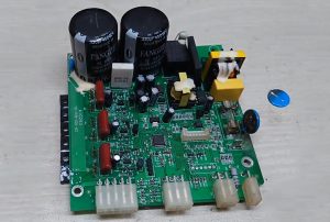
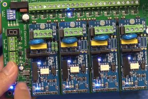
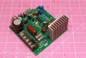
As the core platform for industrial-grade power supplies, the manufacturing and assembly processes for industrial power PCBAs (Printed Circuit Board Assemblies) involve levels of complexity and precision that far exceed those of standard consumer electronics.
The manufacturing of industrial power PCBAs encompasses not only traditional PCB fabrication and component mounting but also a series of complex technical processes, such as heavy copper technology, High-Density Interconnect (HDI) design, high-voltage/low-voltage isolation, thermal management for high-power components, rigorous assembly inspection, and demanding anti-corrosion and insulation coating applications.
A comprehensive analysis of the entire industrial power PCBA workflow—spanning circuit design, material selection, PCB fabrication, component mounting, soldering control, and testing/protection—offers significant engineering value for enhancing the overall quality and market competitiveness of industrial power supply products.
I. Core Design Characteristics and Technical Challenges of Industrial Power PCBAs
High Power Density and Thermal Management Challenges
Industrial power supplies are evolving toward smaller sizes and higher efficiencies, resulting in significantly increased power density. However, high-power components generate substantial heat during operation; if this heat is not effectively dissipated, component junction temperatures can rise excessively, leading to thermal runaway or accelerated component aging.
Consequently, PCB design and assembly must integrate solutions involving heat conduction, convection, and radiation. Techniques such as large-area copper pours, thermal vias, aluminum- or copper-based substrates, and embedded copper blocks are employed to establish efficient thermal dissipation paths.
Mixed High-Voltage/Low-Voltage Circuits and Electrical Isolation
Industrial power PCBAs often integrate high-voltage input/output sections (AC or high-voltage DC) with low-voltage control circuitry (e.g., MCUs, DSPs, PWM controllers) on a single board. Ensuring electrical safety between high-voltage and low-voltage sections is critical; designs must strictly adhere to safety standards (such as UL60950 and IEC62368) by maintaining adequate creepage distances and electrical clearances. Additionally, physical and signal isolation—using optocouplers, digital isolators, or isolation transformers—is employed to prevent high-voltage surges from infiltrating low-voltage control circuits.
Electromagnetic Compatibility (EMC) and Interference Immunity
In industrial environments, the high-frequency switching of high-power transistors generates severe di/dt and dv/dt transients, resulting in intense electromagnetic interference (EMI). Industrial-grade power supply PCBAs must possess excellent electromagnetic susceptibility (EMS) immunity. Design and manufacturing strategies—such as minimizing loop areas, grounding shielding layers, optimizing filter circuit layout, and planning dedicated power/ground shielding planes in multilayer boards—are essential to ensure the system successfully passes conducted and radiated emission tests.
High Reliability and Adaptability to Harsh Environments
Industrial power supplies often require continuous, long-term operation across temperature ranges of -40°C to +85°C (or even wider), while also withstanding mechanical vibration and chemical corrosion. These conditions impose engineering requirements far stricter than those for consumer electronics regarding PCBA solder joint fatigue strength, the matching of the substrate’s Coefficient of Thermal Expansion (CTE), component stress resistance, and the integrity of moisture- and corrosion-resistant conformal coatings.
II. Key Materials and Processes for Industrial-Grade Power Supply PCBs
Selection of High-Performance Substrates
The choice of substrate material for industrial-grade power supply PCBs directly impacts electrical performance and thermal durability:
(1) High-Tg Materials: FR-4 or modified resin substrates with a Glass Transition Temperature (Tg) ≥ 170°C are typically selected to prevent material softening or deformation during continuous high-temperature operation.
(2) High CTI Value: A Comparative Tracking Index (CTI) of 600V (Group I) is required to enhance resistance to tracking failure under high voltage and to reduce necessary creepage distances.
(3) Low-Loss and High-Thermal-Conductivity Substrates: For specific high-power or high-frequency power supplies, metal-core PCBs (MCPCB) or polyimide (PI) substrates are utilized to improve thermal conductivity and dielectric stability.
Heavy Copper Manufacturing Technology
To handle high currents ranging from tens to over a hundred amperes, industrial power supply PCBs often utilize heavy copper boards with weights of 2 oz, 3 oz, or even 6 oz and above. Key challenges associated with heavy copper manufacturing include:
(1) Etching Undercut: Etching thick copper layers is difficult and prone to significant undercut. Precise control of etchant concentration, spray pressure, and etching speed is required, alongside appropriate compensation for trace width and spacing.
(2) Lamination and Resin Filling: Deep channels formed between heavy copper layers are highly susceptible to void formation during multilayer lamination. High-flow prepreg must be used, and heating and pressure profiles optimized, to ensure the resin fully fills the gaps between copper features.
Slotting and High-Voltage Isolation Processing
To meet high-voltage isolation requirements, isolation slots are typically machined into the PCB at the interface between high-voltage and low-voltage sections. Slot machining must ensure smooth edges free of burrs or residual copper; additionally, the subsequent solder mask process must prevent excessive resin accumulation within the slots, which could lead to cracking or delamination.
Solder Mask and Surface Finish Processes
(1) Solder Mask Thickness Control: Applying solder mask to heavy copper boards is challenging. Multiple passes of screen printing or electrostatic spraying are required to ensure the coating thickness at copper corners meets standards, thereby preventing high-voltage breakdown.
(2) Surface Finish Selection: Industrial power supply PCBAs commonly employ Electroless Nickel/Immersion Gold (ENIG), Immersion Tin, or Immersion Silver finishes. For pads intended for high-current power components, ENIG offers a flat surface and excellent oxidation resistance, facilitating the soldering of large SMD components.
III. Industrial-Grade Power Supply PCBA Assembly Processes
Key Technical Controls for Surface Mount Technology (SMT)
(1) Stencil Design and Solder Paste Printing: Industrial power supplies incorporate numerous irregularly shaped, high-power SMD components (such as D2PAK, PQFN, etc.) and high-density packaged chips. Stencil design requires laser cutting and electropolishing processes; grid-style aperture windowing is used for power pads to prevent excessive solder paste from causing component drift or solder balling, while ensuring solder paste coverage exceeds 80% to facilitate heat dissipation.
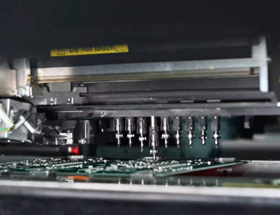
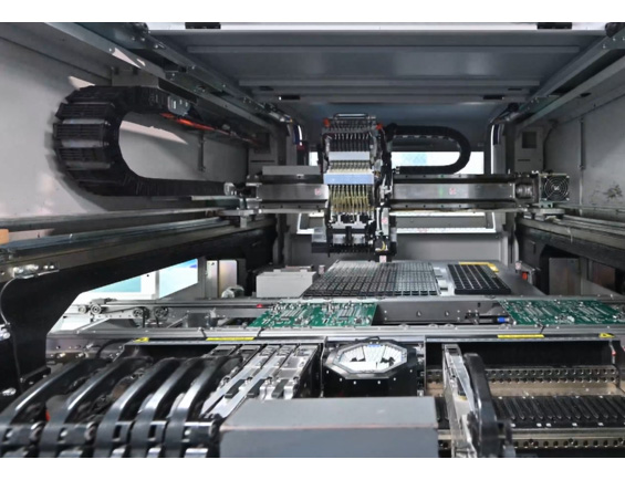
(2) Placement of Irregular and Heavy Components: Industrial power supply boards often feature large surface-mount inductors, high-voltage film capacitors, and heavy power transistors. Pick-and-place machines must possess high-precision image recognition capabilities and adjustable nozzle pressure control to prevent component damage or positional misalignment during placement.
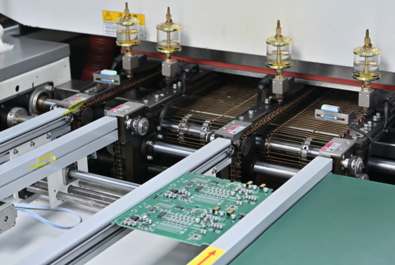
(3) Reflow Soldering Profile Optimization: The presence of thick copper boards and components with high thermal mass results in highly uneven thermal capacity across the board surface. Reflow soldering requires a multi-zone (typically 10–12 zones) nitrogen reflow oven. Temperature settings for preheating, soaking, peak, and cooling stages must be meticulously calibrated to minimize the temperature differential across the board (ΔT ≤ 5°C), ensuring complete melting of high-thermal-mass components without damaging smaller, heat-sensitive ones.
Through-Hole Technology (THT) and Selective Wave Soldering
Industrial power supplies contain a large number of high-capacity electrolytic capacitors, high-frequency transformers, common-mode inductors, terminal blocks, and other high-power through-hole components.
(1) Conventional Wave Soldering vs. Selective Wave Soldering: Conventional wave soldering poses a risk of secondary thermal shock to previously mounted SMD components. Modern industrial power supply manufacturing widely employs selective wave soldering.
Precision CNC nozzles apply flux and solder accurately to through-hole leads, significantly improving the solder fill rate for thick copper boards (achieving over 75% penetration) and reducing the risk of solder joint short circuits.
(2) Manual Soldering and Rework Standards: For specific large or specialized components unsuitable for automated soldering, highly qualified operators must perform manual soldering in accordance with IPC-J-STD-001 standards. High-power, constant-temperature soldering irons supplemented by hot-air preheating are required; defects such as cold joints, solder encapsulation, or copper foil delamination are strictly prohibited.
Stress and Securing Management in Mixed Assembly
Heavy components in industrial power supplies (such as transformers, inductors, and high-voltage capacitors) are highly susceptible to damaging solder joints or tearing PCB copper foil when subjected to mechanical shock or vibration. Therefore, a structural adhesive (e.g., silicone or red glue) securing process must be implemented during assembly; large components are bonded to the PCB via adhesive dispensing and curing to effectively distribute mechanical stress.
IV. Process Quality Control and Inspection Systems
Solder Paste Inspection (SPI) and Automated Optical Inspection (AOI)
(1) 3D SPI: Following solder paste printing, a 3D SPI system precisely measures solder paste volume, thickness, area, and offset, enabling the detection of printing defects prior to the component placement stage.
(2) Pre-reflow/Post-reflow 3D AOI: Pre-reflow AOI primarily checks for incorrect components, missing components, reversed polarity, and placement offsets. Post-reflow AOI focuses on comprehensive inspection of solder joints for wetting angles, bridging, tombstoning, cold joints, and insufficient solder.
X-Ray Inspection
Power components in industrial power supplies (such as DPAK, QFN, and BGA packages) typically feature large exposed thermal pads on their undersides. The void ratio of the solder beneath these pads directly impacts thermal resistance. Using 3D X-ray inspection equipment, the void ratio of the bottom pads on power devices can be precisely calculated (typically requiring a single-void ratio < 10% and a total void ratio < 15%) to ensure heat dissipation performance meets standards.
Flying Probe Testing and In-Circuit Testing (ICT)
ICT utilizes a custom bed-of-nails fixture to contact PCBA test points, rapidly identifying open circuits, short circuits, component tolerances (resistors, capacitors, inductors), and static parameters of diodes/transistors, thereby ensuring the hardware is free of physical defects in an unpowered state.
Functional Testing (FCT) and Burn-In Testing
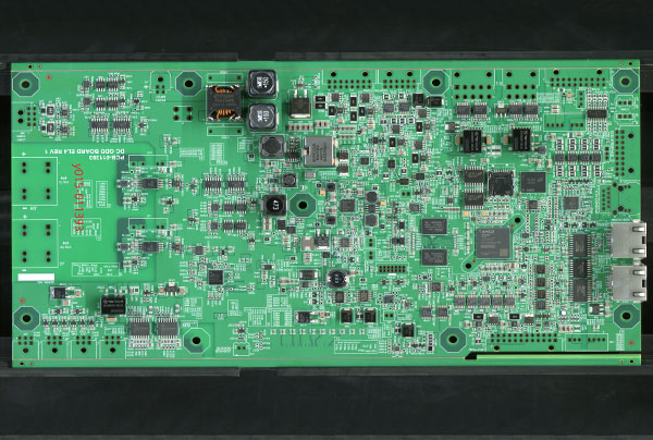
(1) FCT (Functional Testing): An automated testing platform simulating the actual operating conditions of industrial power supplies is used to comprehensively verify electrical specifications, including input voltage range, output voltage accuracy, ripple and noise, conversion efficiency, over-current protection (OCP), over-voltage protection (OVP), and over-temperature protection (OTP).
(2) Dynamic Burn-In Testing (ESS/Burn-In): Industrial-grade power supply PCBAs must undergo rigorous high-temperature dynamic burn-in testing before leaving the factory.
PCBAs are placed in a burn-in chamber at temperatures ranging from 50°C to 85°C and operated continuously for 12 to 48 hours under rated or over-rated loads; a real-time monitoring system is used to screen out products prone to “infant mortality” (early-stage failure).
V. Protection and Post-Processing Technologies
Industrial Conformal Coating Process
Industrial power supplies are frequently exposed to harsh environments containing moisture, salt spray, dust, and corrosive gases. Applying conformal coating (acrylic, polyurethane, or silicone) is an essential step following PCBA assembly and testing:
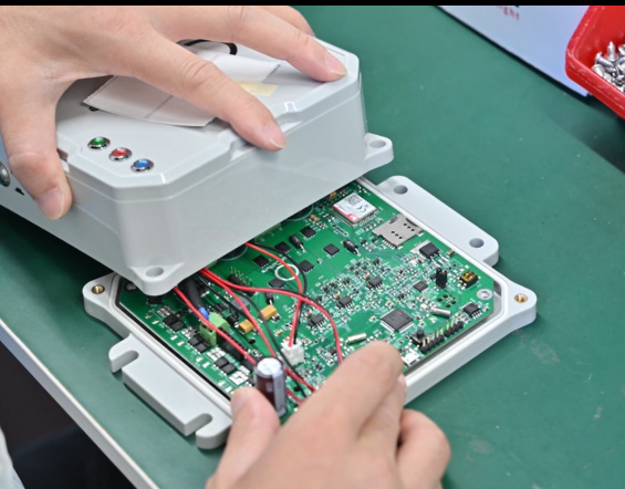
(1) Coating Area Control: Fully automated selective coating machines are employed to strictly avoid coating areas that must remain uncoated, such as terminal blocks, test points, adjustable resistors, and the light-receiving surfaces of optocouplers.
(2) Film Thickness and Curing: Control the film thickness between 30 μm and 130 μm, and employ UV or thermal curing channels for rapid curing; use black light (UV) inspection to verify coating uniformity and coverage integrity.
Potting and Encapsulation Technology
For industrial power supplies operating in extremely harsh environments (such as mining sites, explosion-proof zones, or high-humidity outdoor locations), full or partial resin potting (e.g., using epoxy resin or silicone rubber) is typically employed.
The potting process involves injecting resin in a vacuum environment to completely eliminate internal air bubbles, thereby providing insulation, moisture and shock resistance, and an excellent thermal conduction path.
VI. Summary
The manufacturing and assembly of industrial-grade power supply PCBAs constitute a systems engineering process that integrates materials science, thermodynamics, electromagnetics, and precision manufacturing techniques.
With the advancement of Industry 4.0 and the new energy sector, the application of third-generation semiconductor devices (such as GaN and SiC) in industrial power supplies is becoming increasingly widespread. This trend is driving industrial power supply PCBAs toward higher switching frequencies, smaller footprints, and higher power densities.
In the future, the manufacturing ecosystem for industrial-grade power supply PCBAs will rely increasingly on the deep integration of digital and intelligent technologies:
Intelligent traceability across the entire manufacturing process: Utilizing MES systems to enable full-lifecycle digital traceability of material batches, soldering parameters, inspection data, and burn-in curves for each PCBA.
Widespread adoption of robotic automated assembly: Employing high-precision industrial robots equipped with vision guidance to perform fully automated insertion, securing, and soldering of odd-form high-power components and complex structural parts.
Green manufacturing and low-carbon processes: Promoting the use of lead-free and low-VOC (Volatile Organic Compound) soldering and coating materials, and implementing energy recovery systems during manufacturing and burn-in testing to achieve efficient, precise, and sustainable development in the industrial power supply manufacturing sector.