
As the core terminal component for machine vision and high-precision optical inspection, AI vision cameras present PCB design and manufacturing challenges that far exceed those of conventional electronic products.
Their circuit boards must not only handle the massive data throughput of high-frame-rate raw image signals but also meet stringent requirements for the precise physical alignment of micron-scale image sensors, dynamic thermal balancing, and rigorous electromagnetic compatibility (EMC).
I. Optoelectronic Hybrid PCB Design and High-Density Interconnect (HDI) Architecture
The PCB architecture design for AI vision cameras must balance the conflicting demands of ultra-high-bandwidth transmission and extremely compact physical dimensions.
High-Frequency/High-Speed Signal Layer Stack-up and Impedance Control
Stack-up Design: Utilizes a multi-layer HDI (High-Density Interconnect) structure with blind and buried vias (typically 8–14 layers; 2nd or 3rd-order stacked or staggered vias). High-speed signal layers (such as MIPI CSI-2/Sub-LVDS at the sensor interface or USB 3.2 Gen2/CoaXPress 2.0/10GbE at the system interface) are placed immediately adjacent to solid ground planes.
Impedance Precision: Differential impedance for microstrip and stripline traces is controlled to 90Ω ±5% or 100Ω ±5%. To minimize high-frequency signal attenuation, high-frequency materials with low dielectric constant (Dk) and low dissipation factor (Df)—such as Panasonic Megtron 6 or the Rogers series—are selected for the substrate.
Mechanical Stress Control in the Micron-Scale Sensor Mounting Area
Board Rigidity and Flatness: To prevent focal plane shifts caused by warping or stretching of the CMOS Image Sensor (CIS) chip, the PCB area beneath the sensor must maintain exceptional flatness, with warpage (bow and twist) strictly controlled to <0.3%.
Stress Isolation Slot Design: Mechanical stress relief slots are incorporated around the CIS mounting area to isolate the sensor from physical deformation caused by housing mounting screws or the insertion and removal of cables.
II. Core Manufacturing Processes and High-Precision SMT Assembly
SMT assembly for AI vision cameras involves not only electrical interconnection but also high-precision optomechanical alignment.
Solder Paste Printing and 3D SPI Inspection
Ultra-fine pitch stencils: For BGA and sensor pads with pitches below 0.4mm, step-down electropolished laser stencils or nano-coated stencils are utilized to ensure a solder paste release rate exceeding 85%.
Comprehensive inspection control: 3D Solder Paste Inspection (SPI) monitors solder paste thickness, volume, and offset in real-time, strictly preventing shorts caused by excess solder or cold joints resulting from insufficient solder.
High-Precision CMOS Sensor Placement
Placement accuracy: High-precision placement machines are used to achieve a placement repeatability of within ±10 μm for large-format CIS chips.
Dust prevention and environmental control: Sensor placement and pre-reflow processes must be conducted in a Class 100 cleanroom environment to prevent dust particles from settling on the sensor’s protective glass or pixel array, which could cause dead pixels or black spots.
Reflow Soldering and Precise Thermal Profile Control
Vacuum reflow soldering: A nitrogen-purged vacuum reflow process is employed to keep the voiding rate of BGA and sensor thermal pads below 5%, ensuring rapid heat dissipation for high-power AI computing chips and sensors.
Low-temperature/Zoned temperature settings: Given the sensor’s extreme sensitivity to thermal shock, the reflow temperature profile is optimized (ramp-up rate <2°C/s) to minimize physical damage to the photosensitive array caused by thermal stress.
III. Thermal Design, Thermal Management, and Electromagnetic Compatibility (EMC)
The high computing power of AI chips (such as NPUs/FPGAs) and the significant heat generated by sensors can lead to temperature rises that induce thermal noise, thereby substantially degrading image signal quality (reducing the Signal-to-Noise Ratio, or SNR).
3D Heat Conduction and Thermal Path Configuration
Metal-base and embedded copper processes: Techniques such as copper inlay (filling deep holes with copper) or high-density thermal via arrays are employed directly beneath SoCs/FPGAs and Power Management ICs (PMICs) to conduct heat directly to the device housing.
Thermal Interface Material (TIM) application: Following SMT assembly, automated dispensing equipment is used to apply high-thermal-conductivity (> 6 W/m·K) phase-change materials or thermal pads, establishing a continuous thermal path from the chip through the PCB ground layer to the aluminum alloy housing.
EMC Suppression and Weak Signal Protection
Analog and digital ground isolation: Power supplies for highly sensitive analog sensor circuits are strictly partitioned from high-speed digital circuits, utilizing single-point grounding or bridge grounding for the ground planes.
Shielding can process: Surface-mount metal shielding cans are installed over core computing units and Image Signal Processing (ISP) circuits to block interference from internal high-frequency radiation affecting analog imaging signals.
IV. End-to-End Quality Inspection and Precision Optical Calibration
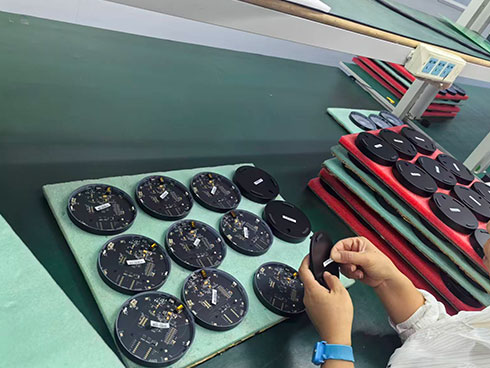
Following assembly, the product must undergo rigorous physical inspection and optical calibration processes to ensure reliability.
Non-Destructive Testing (AOI & 3D X-Ray)
Post-Reflow AOI: Inspects ultra-small components (e.g., 01005/0201 packages) for defects such as tombstoning, misalignment, and skew.
3D X-Ray Inspection: Performs 100% scanning of hidden solder joints—such as the ball grid arrays (BGA) on CIS sensors and high-performance computing (HPC) chips—to detect internal voids, bridging, and cold solder joints.
Active Alignment (AA)
AA Process Implementation: Unlike standard cameras, high-precision AI vision cameras require powered-on calibration. AA equipment captures real-time images to make micron-level adjustments to the relative position of the lens and the PCB-mounted sensor (adjusting X, Y, and Z axes, as well as θₓ, θᵧ, and θz tilt angles).
Optical Axis Locking: Once image clarity (MTF value) and corner-to-corner balance reach optimal levels, UV adhesive is applied and rapidly cured to permanently lock the optical-mechanical structure.
High-Temperature Burn-in and Image Noise Calibration
Burn-in Testing: Assembled products undergo extended (typically 24–48 hours) high- and low-temperature cycling burn-in tests.
Sensor Noise Calibration: Post-burn-in, the system performs dark current correction, flat-field correction (FFC), and defective pixel replacement (DFC) to ensure the camera’s output image purity meets industrial inspection standards.
V. Conformal Coating and Environmental Protection
AI vision cameras are frequently deployed in industrial automation lines, outdoor surveillance, and automotive environments; consequently, the PCB must be resistant to water, dust, salt spray, and chemical corrosion.
Selective Masking for Sensors and Optical Paths
Precision Masking (Keep-out Zone): Prior to the application of conformal coatings (such as acrylic, silicone, or polyurethane), micron-level precision masking or fixture-based protection must be applied to the CMOS sensor cover glass, lens mount, high-speed interfaces (USB/CoaXPress/M12), and thermal interface contact areas; contamination of the optical path by the coating material is strictly prohibited.
Selective Automated Coating: A multi-axis selective coating machine is utilized to precisely control the coating film thickness within the 30 μm – 75 μm range.
Underfill and Mechanical Vibration-Resistant Bonding
BGA/SoC Underfill Process: For core AI computing chips (e.g., NPUs, FPGAs) and the BGA solder joints beneath sensor packages, a low-CTE (Coefficient of Thermal Expansion) epoxy resin is applied via underfill dispensing and heat curing, significantly enhancing resistance to impact and thermal cycling fatigue.
Bonding of Large Components: Heavy components susceptible to vibration—such as electrolytic capacitors and large inductors—are secured at their bases using industrial-grade silicone (RTV) to prevent solder pad cracking caused by high-frequency vibration.
VI. Industrial-Grade Environmental Reliability Verification and Physical Stress Testing
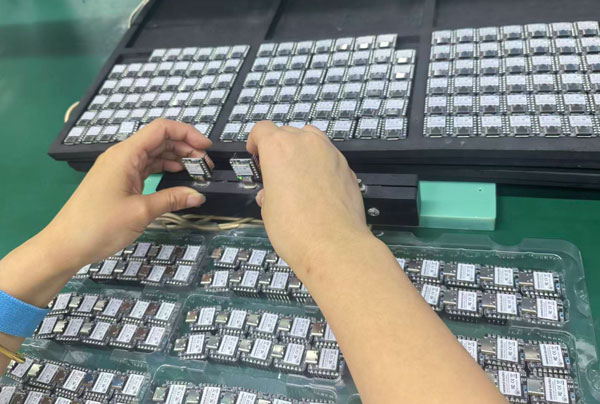
Assembled PCB assemblies (PCBAs) must undergo comprehensive Environmental Stress Screening (ESS) to ensure zero defects upon shipment.
Environmental and Thermal Stress Screening
Thermal Shock Test: Hundreds of rapid cycles are performed between temperature extremes of -40°C and +85°C to detect micro-cracks or cold solder joints resulting from mismatches in the coefficients of thermal expansion among various materials (FR-4, copper foil, silicon chips, and solder).
Damp-Heat Aging (HAST / THB): “Double 85” (85°C temperature / 85% humidity) powered operation testing to verify PCB ion migration (CAF effect) and the protective efficacy of conformal coatings.
Mechanical and Structural Reliability
Random Vibration & Mechanical Shock: Simulates industrial robotic arm and vehicle operating environments (5G–50G acceleration) to detect issues such as loose structural screws, fractured solder joints, and optical axis misalignment.
Drop and Electrostatic Discharge (ESD) Testing: Conducts ESD immunity testing at ±8kV (contact discharge) and ±15kV (air discharge) to safeguard sensitive image acquisition circuitry.
VII. AI Vision Camera PCB Assembly Factory
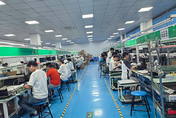
KingTop Technology is a global supplier specializing in high-precision PCB manufacturing and advanced Electronics Manufacturing Services (EMS). Backed by a 10,000-square-meter modern cleanroom production facility, over 11 fully automated SMT lines, and a professional team of more than 260 engineers and production staff, KingTop offers a fully integrated, one-stop solution for AI vision camera PCB assembly and manufacturing—encompassing bare board fabrication, precision SMT placement, optical calibration, and environmental testing.
Manufacturing Foundation Aligned with AI Vision Production Capabilities
Large-Scale Hardware Infrastructure
10,000 m² Modern Cleanroom Facility: Features dedicated Class 100 and Class 1000 clean zones to completely eliminate dust contamination on CMOS Image Sensor (CIS) pixel arrays and optical protective glass.
11+ Fully Automated SMT Lines: Equipped with high-precision placement machines, 3D SPI (Solder Paste Inspection) systems, and vacuum reflow soldering equipment; offers flexible production capacity to handle both rapid prototyping (NPI) and high-volume contract manufacturing needs. Deployment of a Professional Technical Team
Support from a team of 260+ professionals: Includes senior DFM/DFA engineers, optoelectronic calibration experts, and an IPC-certified quality team. They engage with customer designs at the early engineering stage to mitigate failure risks associated with complex HDI boards and sensor board assemblies.

KingTop’s Core Technical Strengths in AI Vision Cameras
Advanced HDI Manufacturing and High-Frequency/High-Speed Material Processing
High-Density Interconnect (HDI) Capabilities: Supports the manufacturing of 8–14 layer boards with 2nd or 3rd-order blind and buried vias, achieving micron-level laser microvias and fine-line circuitry (3mil/3mil spacing).
Precision Impedance and Material Selection: Fully utilizes high-frequency, low-loss substrates such as Megtron 6 and Rogers, strictly controlling differential impedance precision to within 5% for image transmission interfaces (MIPI CSI-2, CoaXPress 2.0, 10GbE).
Micron-Level CMOS Sensor Mounting and Active Alignment (AA)
High-Precision CIS Mounting: Employs module placement equipment with a repeatability of ±10μm, ensuring the flatness and alignment of large-format image sensors during the SMT process.
Integrated Opto-Mechanical-Electrical Calibration: Utilizes a high-precision Active Alignment (AA) system to dynamically fine-tune the 6-DOF (degrees of freedom) spatial relationship between the lens and sensor while powered on, achieving high MTF (Modulation Transfer Function) optical imaging across the entire field of view.
High-Quality Thermal Management and Reliable Packaging
Vacuum Reflow Soldering: A vacuum reflow process with nitrogen protection keeps the voiding rate for BGA and SoC/NPU thermal pads below 5%, significantly reducing thermal resistance for high-performance computing chips.
Underfill and Selective Coating: Equipped with 3-axis automatic dispensing machines and selective coating lines, the process applies underfill to core BGA components and performs selective conformal coating on sensitive circuit areas to withstand vibration and moisture corrosion in industrial environments.
Summary
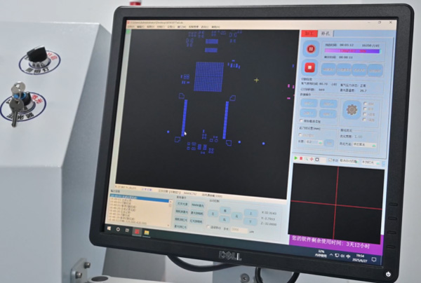
The PCB assembly and manufacturing of AI vision cameras constitute a systems engineering process that integrates high-frequency/high-speed circuit design, micron-level opto-electro-mechanical alignment, efficient thermal management, and high-reliability protective coating.
Design Phase: High-order HDI stack-up and stress-isolation designs are employed to address high-speed signal integrity (SI) and mechanical deformation of the sensor.
Manufacturing Phase: Class 100 cleanroom SMT, vacuum reflow soldering, and Active Alignment technologies ensure precise optical path alignment and low-noise image acquisition.
Protection Phase: A combination of underfill, selective coating, and rigorous environmental stress testing ensures the device’s long-term stability in harsh industrial environments.