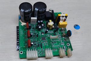
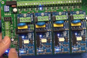
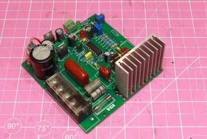
Centered on high-density interconnect (HDI) technology, high-speed signal management, and end-to-end reliability verification, these solutions provide comprehensive support—from collaborative design to mass production delivery—for edge-based visual computing hardware.
I. PCB Design: The “Neural Network Skeleton” of AI Cameras
The PCB of an AI camera is not a conventional circuit board; rather, it is a multi-layer, heterogeneous integration platform that combines high-speed signal transmission, high-density interconnects, and precise thermal management. Its design focuses primarily on “computing density” and “signal fidelity.”
| Design Dimension | Technical Requirements | Industry Practice |
| Layer Stackup | 8–20 layers, including dedicated power and ground planes | Adopt a “Signal–Power–Ground–Signal” alternating stackup to reduce return-path length |
| Impedance Control | Differential impedance: 100 Ω ± 5%; single-ended impedance: 50 Ω ± 5% | Use HFSS simulation to dynamically adjust trace width and interlayer spacing, ensuring eye-diagram opening >70% |
| High-Speed Routing | Differential-pair length matching tolerance ≤5 mil; avoid 90° corners | Use serpentine trace compensation for clock signals to avoid crossing split planes |
| Material Selection | Base material: high-Tg FR-4 (Tg ≥170°C); high-speed regions: Rogers 4350B or ceramic-filled laminate | Use standard-area FR-4 (Dk 4.5–5.5); use ceramic substrates (Dk 9–10) for RF modules |
| Thermal Design | Local copper thickness ≥2 oz; thermal-via density ≥15 vias/mm²; copper-inlaid structure | Arrange thermal-via arrays beneath BGA packages and connect them to bottom-layer heat-spreading copper foil, reducing thermal resistance by 40% |
| Microvia Process | Laser-drilled microvias (hole diameter ≤80 μm); stacked microvias (ALIVH) | Implement fan-out routing for BGA pitches below 0.3 mm, increasing routing density by 300% |
Physical Foundation: When the PCB is powered, current flows along copper traces; vias establish interlayer connectivity, while pads serve as the mechanical and electrical connection points between component leads and the copper foil. As voltage rises, the density of charge carriers increases and LED brightness intensifies synchronously, intuitively demonstrating the fundamental nature of the “current path.”
II. PCBA Assembly: Precision Manufacturing from Solder Paste to Functional Modules
PCB assembly for AI cameras is an industrial art form requiring micron-level precision and millisecond-level timing control; the core processes are as follows:
Complete SMT Assembly Process (Including Key Parameters)
| Process Step | Equipment / Process | Key Parameters | Quality Standards |
|---|---|---|---|
| Solder Paste Printing | Stencil Printer | Stencil thickness: 0.10–0.15 mm; printing thickness tolerance: ≤ ±10% | Pad coverage ≥ 90% |
| Component Placement | High-Speed Pick-and-Place Machine | Placement accuracy: ±0.05 mm for 0402 components; BGA ball diameter tolerance: ±20% | Polarity component orientation error ≤ 1° |
| Reflow Soldering | Nitrogen-Protected Reflow Oven | Temperature profile: preheating 150–180°C (120 s); peak temperature 235–250°C (60 s); cooling rate > 1.5°C/s | BGA void ratio ≤ 25% (Class 3) |
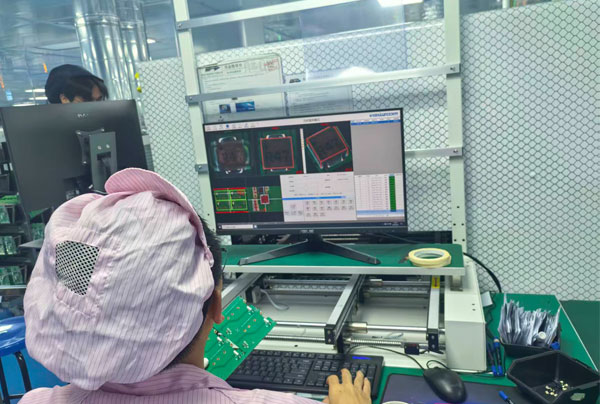
| AOI Inspection | 3D Confocal Optical Inspection System | Resolution: 20 μm; deep-learning defect classification F1-score ≥ 0.98 | Detects 13 types of defects, including insufficient solder / cold solder joints, tombstoning, solder balls, component misalignment, etc. |
2. Quality control standard: IPC-A-610 Class 3
| Inspection Item | Class 3 Requirements (AI Camera Applicable) | Inspection Method |
|---|---|---|
| Solder Joint Wetting | Solder coverage of leads ≥ 75%; contact angle < 90°; no non-wetted areas | Optical Microscope (20–100×) |
| Solder Volume | Solder coverage on the terminations of SMD components ≥ 75%; through-hole fill rate 100% | X-Ray Computed Tomography (CT) |
| BGA Solder Joints | Void ratio ≤ 25%; no cracks or solder bridges | Microfocus X-Ray (5 μm resolution) |
| Visual Defects | Reject solder balls > 0.13 mm, solder spikes, and solder splatter | Manual Inspection + AOI Dual Inspection |
Process Breakthroughs: A digital twin system is employed to predict welding defects, reducing debugging time by 30%; selective wave soldering is used for mixed-assembly processes, cutting chemical residues by 90%.
III. Key Technical Challenges and Engineering Solutions
Conflict between High-Density Interconnect (HDI) and Thermal Management
| Challenges | Causes | Solutions |
|---|---|---|
| Trapped Heat | The thermal conductivity of FR-4 is only 0.3 W/m·K, while that of the resin used for microvia filling is < 1 W/m·K | Use copper-filled microvias with thermal conductivity > 400 W/m·K; locally embed copper foil heat-spreading layers |
| Interlayer Registration Error | Cumulative error exceeds 10 μm in PCBs with more than 16 layers, potentially causing open circuits in blind vias | Use laser reference points + machine-learning compensation algorithms to control cumulative error to ≤ 5 μm |
| BGA Soldering Failure | Coefficient of thermal expansion (CTE) mismatch between the chip (Si) and PCB (FR-4) | Apply underfill; optimize the reflow temperature profile to reduce peak thermal stress |
Signal Integrity and Power Supply Noise Suppression
| Problem | Impact | Solution |
|---|---|---|
| Clock Jitter | Causes image sampling distortion, leading to AI inference errors | Use an independent LDO power supply; ground the shielding layer of clock traces; use a low-phase-noise crystal oscillator (<1 ps RMS) |
| Power Supply Noise | Affects ADC sampling accuracy and reduces the image signal-to-noise ratio (SNR) | Design a π-type filter network (100 μF tantalum capacitor + 10 Ω + 0.1 μF); partition the power plane to avoid cross-interference |
| Crosstalk | High-speed data lines interfere with video signals | Increase spacing to more than 3× the trace width; use ground isolation strips; route differential pairs to avoid parallel coupling |
Design for Manufacturability (DFM) and Design for Testability (DFT)
| Design Principles | Implementation Guidelines | Value |
|---|---|---|
| DFM | Extend pads by 20% to facilitate solder wicking; avoid QFN packages smaller than 0.3 mm; standardize component orientation | Reduce rework rate by 60%; increase mass-production yield to 98%+ |
| DFT | Implement a JTAG boundary-scan chain; add test points at critical nodes; reserve probe access channels in BGA areas | Achieve >95% test coverage; reduce fault isolation time by 70% |
Collaborative Design: DFM and DFT must be integrated at the RTL stage to avoid the cost trap of board redesigns after the design is finalized—industry data shows that the cost of corrections during the design phase is only one-tenth of that during mass production.
IV. Industry Practices and Customized Service Models (Shenzhen as a Hub)
As a global hub for AI camera manufacturing, Shenzhen’s PCBA customization ecosystem exhibits three key characteristics:
| Model | Representative Companies | Service Characteristics | Delivery Time |
|---|---|---|---|
| Modular Customization | KingTop Technology, Shenzhen Luxshare, Han’s Laser | Provides an “AI Camera Core Module” integrating the SoC, memory, and camera-interface PCBA; customers only need to integrate the lens and enclosure | 7–10 days (small batches) |
| High-Reliability Contract Manufacturing | Shennan Circuits, KingTop Technology, Kinwong Electronic | Focuses on Class 3 standards and holds ISO 13485 (medical-grade) and IATF 16949 (automotive-grade) certifications | 15–20 days |
| Rapid Prototyping Platform | KingTop Technology, JLCPCB, Jieduobang | Supports 0.1 mm microvias, 64-layer boards, and impedance control; online ordering with samples available within 24 hours | 3–5 days |
Case Study: Certain DJI AI drone camera modules utilize a structure featuring a ceramic substrate, embedded copper, and laser blind vias to achieve low-latency transmission of 1280×1024@120fps video streams, with a stable PCBA yield of 97.2%.
V. Current Technical Bottlenecks and Future Trends
| Bottleneck | Current Status | Breakthrough Direction |
|---|---|---|
| Thermal Density Limit | Local power density of the SoC reaches 30 W/cm² | Adopt 2.5D/3D packaging, vertically stacking AI chips and memory to shorten interconnect paths |
| Material Cost | High-frequency ceramic substrates cost 8–10 times more than FR-4 | Develop low-loss composite materials (e.g., PTFE + fiberglass) |
| Testing Complexity | BGA solder joints are invisible, making defects difficult to locate | Promote AI-driven automated X-ray image analysis systems, with detection accuracy >99% |
| Green Manufacturing | Lead-free solder has a high melting point and consumes significant energy | Develop low-temperature solder paste (melting point <180°C) and water-based cleaning processes |
Trend Forecast: By 2027, AI-assisted PCB design tools (such as Altium Designer AI plugins) are expected to become widespread, automatically optimizing impedance, thermal management, and DFM, while reducing design cycles by 50%.
VI. Conclusion: The Engineering Philosophy of AI Camera PCBA
AI camera PCB assembly and PCBA customization are, at their core, about balancing four competing priorities at the micron scale: performance, reliability, cost, and manufacturability.
Design is the soul: Without DFM/DFT, a PCB is merely “theoretical planning without practical execution.”
Process is the muscle: Without nitrogen reflow and 3D AOI on the production line, the manufacturing process is like “a blind man trying to understand an elephant.”
Standards are the skeleton: Without the constraints of IPC-A-610 Class 3, the result risks becoming a “substandard construction project.”
In Shenzhen, a global manufacturing hub, AI camera PCBA has evolved from “contract assembly” to “system-level collaborative innovation.” Its technological depth extends far beyond the traditional consumer electronics sector, and it is becoming a core infrastructure for the era of intelligent vision.