In an era where optical sensing, 3D vision, and AI hardware are deeply integrated, depth cameras have transitioned from the laboratory into core sectors such as industrial automation, intelligent robotics, autonomous driving, biometrics, and 3D reconstruction.
As the central hub of the depth camera’s hardware architecture, the PCBA (Printed Circuit Board Assembly) not only handles electrical signal transmission and power management but also directly determines data throughput efficiency for optical sensors, clock synchronization precision, thermal stability, and overall image quality.
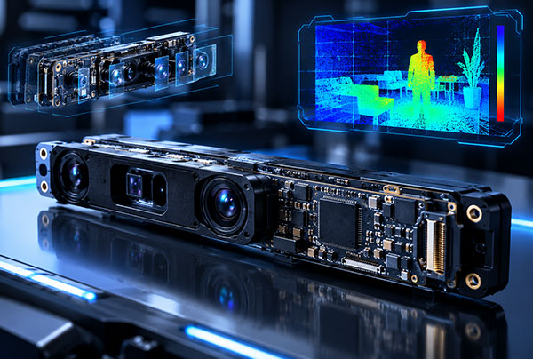
Because depth cameras typically integrate high-resolution image sensors (such as CMOS or ToF sensors), VCSEL/LED infrared light sources, dedicated Image Signal Processors (ISPs), FPGA/ASIC chips, and high-speed transmission interfaces, their PCBA design and manufacturing processes differ fundamentally from those of standard electronic products.
Conventional PCB assembly workflows struggle to meet the rigorous challenges posed by optical alignment precision, high-frequency differential signal integrity, high-power-density thermal management, and microsecond-level multi-sensor synchronization. Consequently, custom depth camera PCBA manufacturing and assembly services have become a critical pillar in accelerating the deployment and mass production of 3D vision hardware.
This article provides a systematic overview of the entire manufacturing chain for depth camera PCBAs—from design and fabrication to high-quality delivery—covering technical architectural features, manufacturing process challenges, core production controls, quality inspection systems, and industry application scenarios.
I. Core Technical Architecture and Design Features of Depth Camera PCBAs
Depth cameras are typically built upon various 3D imaging principles; mainstream solutions include Structured Light, Binocular Stereo Vision, and Time-of-Flight (ToF). The specific imaging principle employed directly dictates the complexity of the PCBA circuit design and the associated manufacturing process requirements.
High-Speed Signal Transmission and Multi-layer High-Density Interconnect (HDI)
Depth cameras must output massive amounts of point cloud data and high-frame-rate depth maps in real-time; consequently, their mainboards often integrate high-speed data interfaces such as MIPI CSI-2, USB 3.1 Gen2, GigE Vision, or PCIe.
Signal Integrity (SI) Control: In PCBA design and manufacturing, high-speed differential signal pairs require precise impedance matching (typically 90Ω or 100Ω). Even minor deviations in trace width, fluctuations in dielectric thickness, or via stubs can lead to signal attenuation, crosstalk, or EMI issues.
HDI Materials and Blind/Buried Via Technology: To accommodate main control chips (such as FPGAs or SoCs) and peripheral circuitry within compact hardware spaces, depth camera PCBAs commonly utilize High-Density Interconnect (HDI) structures. These incorporate first-order, second-order, or even “Any-layer” blind and buried via technologies to facilitate high-density BGA pin breakout.
Precision Clock Synchronization and Triggering Circuits
For binocular camera or infrared structured light systems, the time difference between image capture from the left and right perspectives must be controlled at the microsecond or even nanosecond level.
Low-Jitter Clock Networks: The PCBA circuitry requires high-precision active crystal oscillators and clock distribution chips; signal traces must maintain strict length matching and symmetry to minimize phase skew.
Hardware Triggering Loops: Absolute synchronization is required between the infrared light emission unit (e.g., VCSEL driver circuit) and the CMOS image sensor’s shutter operation. The switching driver circuits on the PCBA must exhibit extremely high response speeds (featuring nanosecond-scale steep rising edges), imposing rigorous manufacturing requirements for controlling localized parasitic inductance and capacitance.
High Power Density and Thermal Management Structures
Whether dealing with the continuously modulated light source of a ToF camera or the projection laser module of a structured light system, the light source driver sections handle high instantaneous currents and generate concentrated heat.
Board-Level Thermal Design: PCBA designs often incorporate metal-core substrates (such as aluminum or copper bases), high-thermal-conductivity heat sinks, copper inlays, or extensive thermal via arrays to rapidly conduct heat generated by optoelectronic components and driver chips toward the structural housing.
Thermal Stress and Deformation Control: Optical sensors are extremely sensitive to minute physical warping of the PCB caused by thermal expansion. Matching the substrate’s Coefficient of Thermal Expansion (CTE) with the sensor packaging materials is critical for both substrate selection and the soldering process.
II. Key Process Challenges in Custom Manufacturing of Depth Camera PCBAs
Compared to standard consumer electronics PCBAs, the custom assembly of depth camera PCBAs presents numerous unique process challenges during actual production.
[High-precision printing/SMT] ──> [Low-residual-stress reflow soldering] ──> [AA Active Alignment/Packaging assembly] ──> [Conformal coating & optical testing]
Image Sensor Placement and Cleanliness Control
CMOS/ToF sensors are among the most valuable components on the PCBA; any particulate contamination or scratching on the protective cover glass or photosensitive area directly results in imaging defects or pixel failure.
Class 100/1000 Cleanroom Environment: Sensor placement and subsequent assembly processes must be conducted in a high-cleanliness cleanroom equipped with laminar flow hoods and HEPA filtration systems.
Coplanarity and Tilt Control: During the placement of sensor bases or chips, the placement machine requires micron-level positioning accuracy (X/Y/Z axes and rotation angle) to ensure exceptional parallelism between the photosensitive surface and the PCB substrate, laying the foundation for subsequent optical lens assembly.
Soldering of Fine-Pitch BGA and Wafer-Level Packages (CSP/WLCSP)
Depth camera main controllers widely utilize high-density BGA and CSP packaged chips, typically featuring pin pitches of less than 0.4mm.
Stencil Aperture Design and Solder Paste Printing: For micro-pads, stencils require laser cutting combined with electropolishing or nano-coating processes to ensure highly uniform solder paste release, thereby preventing bridging shorts or “tombstoning.”
Reflow Profile Optimization: Since the board contains both high-thermal-mass components (such as metal heat sinks or power modules) and heat-sensitive optical components, the reflow profile requires precise calibration of the heating rate, soak phase, and cooling rate. This prevents thermal stress from causing board warpage or pad cracking.
Active Alignment (AA) Integration for Optical Modules
Although the AA process is often categorized as part of module packaging, the PCBA serves as the physical and electrical platform for the AA alignment process.
Substrate Flatness Control: The surface flatness of the PCBA in the optical interface area must be strictly controlled. Even slight distortion of the PCB after soldering can cause the lens holder to tilt upon installation, leading to optical axis misalignment and severely compromising the stereo matching accuracy of depth algorithms.
Structural Bonding and Curing: Attaching the optical lens holder to the PCBA typically involves dispensing an adhesive (such as UV-curable or low-temperature heat-curable glue). Parameters such as the adhesive’s curing shrinkage rate, dispensing volume, and curing temperature profile must be rigorously validated to prevent curing-induced stress from shifting the sensor’s position.
III. From Design to Delivery: The End-to-End Process of Custom Depth Camera PCBA Assembly
Custom depth camera PCBA manufacturing is not merely a simple “contract assembly” task; it is a comprehensive system engineering process encompassing Design for Manufacturability (DFM) analysis, supply chain management, precision assembly, and comprehensive testing.
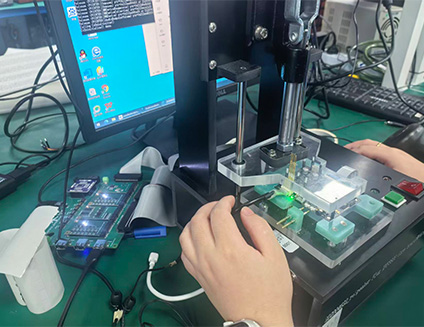
DFM (Design for Manufacturability) and DFA (Design for Assembly) Pre-review
Before entering mass production, the manufacturing team conducts a thorough review of the client-provided PCB Gerber files, Bill of Materials (BOM), and assembly drawings:
Impedance Control and Stack-up Verification: Verifying the dielectric layer thickness and reference plane integrity for high-frequency signal lines.
Component Spacing and Pad Design: Evaluating the placement of decoupling capacitors around BGA components to ensure high-precision SMT placement heads do not encounter mechanical interference; optimizing the layout of thermal vias for high-heat components.
Test Point Coverage: Strategically incorporate ICT (In-Circuit Test) or FCT (Functional Test) points within the circuit network to ensure the measurability of circuit continuity and voltages at critical nodes.
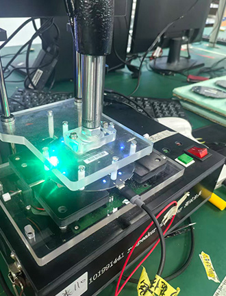
Raw Material Procurement and Quality Control (BOM Supply Chain)
Depth cameras utilize numerous specialized or high-specification optoelectronic components, dedicated power management ICs (PMICs), and high-precision passive components.
Component Traceability: Critical semiconductor devices and optical sensors must be procured directly from original manufacturers or authorized distributors; strict controls regarding ESD (Electrostatic Discharge) protection and MSD (Moisture-Sensitive Device) baking must be implemented.
High-Specification PCB Substrate Customization: Utilize high-Tg (e.g., Tg > 170°C), low-Dk (dielectric constant), and low-Df (dissipation factor) materials—such as those from Shengyi (including halogen-free options), Rogers, or the Panasonic Megtron series—to ensure dimensional stability during high-temperature processing and high-frequency signal transmission.
Precision SMT Assembly and Soldering Processes
The table below outlines the core processes and corresponding control standards for depth camera PCBA manufacturing:
| Process Stage | Key Control Element | Technical Specifications / Quality Standard |
| Solder Paste Printing | 3D SPI thickness & volume inspection | Shape integrity > 95%, volume deviation controlled within ±10% |
| Precision SMT Placement | Image sensor & high-density BGA positioning | X/Y alignment accuracy ±10µm, precise closed-loop control of placement force |
| Nitrogen Reflow Soldering | Chamber oxygen concentration & temperature profile | Nitrogen environment ($O_2$ content < 500ppm), reducing solder joint oxidation and voiding rate |
| AOI Inspection | 100% 3D AOI inspection | Full scanning for wrong parts, missing components, reversed polarity, cold joints, bridging, etc. |
| X-Ray Inspection | Bottom voiding rate for BGA/QFN/image sensors | Voiding rate controlled below 10%–15% |
Dispensing, Conformal Coating, and Underfill Processes
To ensure the reliability of the depth camera under conditions such as industrial vibration, automotive jolts, or fluctuating high and low temperatures:
BGA Underfill: High-flowability epoxy resin is injected beneath high-stress BGA components and sensors; thermal curing is then used to enhance the solder joints’ resistance to mechanical shock.
Selective Conformal Coating: Automated spraying is applied to designated protective areas—while carefully avoiding optical sensing regions, connector contacts, and heat dissipation surfaces—to provide protection against moisture, salt spray, and dust.
IV. Quality Assurance System and Specialized Testing
The hardware quality of the depth camera determines the positioning accuracy and operational stability of the entire vision system; consequently, its testing procedures are more rigorous than those for standard electronic products.
Automated Electrical Testing (ICT and FCT)
ICT (In-Circuit Test): A bed-of-nails fixture is used to rapidly check the PCBA for open/short circuits, resistance and capacitance values, and basic IC logic functions, thereby screening out fundamental manufacturing defects.
FCT (Functional Test) & Firmware Programming: Firmware is programmed into the main control chip, followed by testing of power rail voltage sequencing, clock signal frequency, MIPI/USB interface data link connectivity, and the current response speed of the infrared drive circuit.
Preliminary Image and Optical Testing (Pre-Optical Test)
Before the complex lens module is installed, the electrical imaging performance of the sensors themselves undergoes preliminary screening:
Bad Pixel and Dark Current Detection: Sensor noise levels are tested in a darkroom environment to identify and reject defective chips.
Light-Emitting Unit (VCSEL/Laser) Electro-Optical Conversion Test: Power consumption and response of the infrared emission circuit are monitored to prevent optical components from burning out due to excessive current.
High/Low-Temperature Aging and Thermal Stability Testing
Burn-in Aging Test: The PCBA is placed in an environmental test chamber and operated continuously under full load at high temperatures (e.g., 60°C–85°C) for 24 to 72 hours to trigger and eliminate components prone to early-stage failure (infant mortality).
Thermal Deformation Monitoring: Monitors electrical drift and physical board warping in the PCBA during prolonged operation at high temperatures, ensuring the validity of subsequent depth camera algorithm calibrations across various temperature gradients.
V. Key Application Areas for Custom Depth Camera PCBA Services
Professional custom assembly services for depth camera PCBAs offer differentiated hardware manufacturing solutions tailored to the specific needs of various vertical sectors:
Industrial Automation and Mobile Robots (AMR/AGV)
Requirements: Exceptional vibration resistance, wide operating temperature range (-40°C to 85°C), and long service life.
Manufacturing Focus: Enhanced underfill processes; use of high-Tg (glass transition temperature) PCB materials and industrial-grade components; reinforced surge protection for power interfaces.
Facial Recognition Payment and Biometric Terminals
Requirements: Extremely compact structure with strict module size constraints; necessitates tamper-proofing and high-level security.
Manufacturing Focus: Multi-layer micro-via HDI structures; tight integration of sensor mounting with optical interfaces; enhanced localized ESD (Electrostatic Discharge) protection.
3D Scanning and Medical Aesthetic Equipment
Requirements: Ultra-high resolution and sub-millimeter depth measurement accuracy; extreme sensitivity to signal noise.
Manufacturing Focus: Strict isolation of analog and digital circuit grounds; use of low-noise LDO power supplies; optimized signal routing with ground shielding.
Automotive Intelligence and Driver/Occupant Monitoring Systems (DMS/OMS)
Requirements: Compliance with automotive-grade quality standards (e.g., IATF 16949); ability to withstand harsh in-vehicle environments and long-term high-load operation.
Manufacturing Focus: Full-process component traceability; “Zero Defect” quality control; rigorous thermal cycling and vibration testing.
VI. Summary and Outlook
Custom manufacturing and assembly of depth camera PCBAs is far more than simple component soldering; it is a high-barrier-to-entry manufacturing service that integrates high-frequency/high-speed circuit design, precision optical assembly, microelectronics packaging, and rigorous thermal management. From impedance matching and thermal layout during the initial DFM review to clean-room SMT assembly and low-stress reflow soldering during manufacturing, and finally to rigorous functional and thermal stability testing—every manufacturing detail directly impacts the imaging performance and operational stability of the final 3D vision system.
Selecting a custom assembly partner with extensive experience in manufacturing optical sensing hardware, high-precision SMT production lines, and a comprehensive QA management system is crucial for accelerating the hardware development and deployment of depth cameras, improving mass production yields, and ensuring market competitiveness.