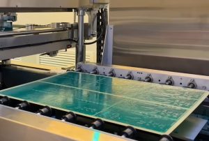
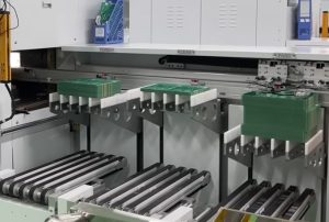
PCB assembly services for AI smart terminals and wearable devices require comprehensive electronic manufacturing solutions ranging from high-quality PCB fabrication, precise SMT & DIP assembly to supply chain management. As a professional PCB assembly factory in China, KingTop Technology provides you with the following guidance.
As edge AI computing power rapidly decentralizes and smart wearables evolve from standalone functional devices into “all-scenario health interaction terminals,” many hardware R&D teams focus heavily on algorithm optimization, chip selection, and industrial design. Yet, they often overlook a critical link that determines final product reliability and the success of mass production: PCB assembly.
For products such as AI smartwatches, AR glasses, and medical-grade wearable monitors, PCB assembly is no longer a simple process of mounting components onto a PCB based on Gerber files using standard SMT lines. Instead, it has become a complex system engineering task involving the placement of high-density micro-components, high-speed signal integrity control, reliability reinforcement for irregularly shaped thin boards, and comprehensive quality control throughout the process.
In Shenzhen—the global hub of electronics manufacturing—many AI device startups share a common experience: prototypes function perfectly, and manually soldered boards run without issues; however, once small-batch trial production (in the hundreds or thousands of units) begins, problems arise—such as cold solder joints, hidden BGA soldering defects, sensor data drift, and solder joint cracking during drop tests. Often, the root cause lies not in the design files, but in the choice of an SMT factory accustomed to standard consumer electronics motherboards; their manufacturing processes are simply ill-suited to the unique requirements of AI smart terminals and wearables. A service provider capable of successfully handling PCB assembly for such complex products must establish a dedicated technical system covering hardware infrastructure, core process expertise, full-chain management, and R&D collaboration capabilities.
I. Why Standard SMT Processes Fail to Meet the Needs of AI Smart Terminals and Wearables
Many people still view PCB assembly in basic terms—simply mounting and soldering components onto a board—believing that high-precision placement machines alone guarantee a quality product. However, manufacturing AI smart terminals and wearables presents a systemic challenge arising from the convergence of multiple constraints: spatial limitations, performance requirements, reliability standards, and scenario-specific adaptability. The general-purpose process systems found in standard consumer electronics SMT factories are fundamentally incapable of meeting these demands.
The first major challenge stems from high-density integration within extremely tight spatial constraints. Smartwatch motherboards are often compressed into a tiny footprint of just 3–5 square centimeters; AR glasses require motherboard circuitry within the temple arms to conform to curved designs; and many medical-grade wearables utilize rigid-flex PCB technology. Within such limited space, engineers must integrate edge AI processors, multiple MEMS sensors, Bluetooth/Wi-Fi communication units, battery management chips, and dozens of 01005-sized micro-passive components (resistors and capacitors), with component spacing reduced to the 0.2mm range.
For standard SMT facilities, the most common issue with these ultra-thin, irregularly shaped boards is thermal warping during reflow soldering. This leads to cold solder joints, component misalignment, or even pads detaching entirely from the substrate. Such problems rarely surface during the initial prototype stage (involving only a few dozen units); instead, they often erupt en masse during small-batch pilot runs of hundreds of units, directly delaying the product’s time-to-market.
The second challenge stems from signal integrity requirements driven by high-speed AI computing power. Edge computing chips in AI-enabled devices must perform real-time AI inference with minimal power consumption, utilizing internal high-speed buses that operate at gigahertz (GHz) frequencies. Densely packed circuit traces are highly susceptible to issues such as signal crosstalk, excessive impedance deviation, and excessive power supply ripple.
Without targeted process controls during PCB assembly, even a design that perfectly adheres to high-speed circuit specifications can result in finished boards plagued by latent defects—such as unstable AI module performance, high packet loss in wireless communication, or excessive sensor sampling errors. These issues often escape detection during final factory inspections, only surfacing after weeks or months of user operation, thereby exposing the brand to significant after-sales risks.
The third challenge arises from the extreme reliability requirements inherent to wearable usage scenarios. Wearable devices are designed for prolonged close contact with the human body and must withstand complex operating conditions, including rapid temperature fluctuations, corrosion from salty sweat, accidental drops and impacts, and repeated flexing in flexible zones. Many users wear smartwatches during exercise, exposing the device to saline sweat; outdoor use involves temperature swings ranging from -5°C to 45°C; and daily handling inevitably includes accidental drops from heights of up to 1.5 meters.
If solder joint strength is insufficient, underfill application is inadequate, or conformal coating is not applied to standard during PCB assembly, products are highly prone to issues such as solder joint cracking, component detachment, and circuit corrosion after just six months of use. A major reason for the poor user experience of many low-cost smart wearable products on the market is the lack of reliability control during the PCB assembly stage.
It is the convergence of these three challenges that has turned PCB assembly for AI smart terminals and wearable devices into a highly demanding niche within the electronics manufacturing sector. Without long-term process expertise and targeted equipment investment, standard SMT factories simply cannot reliably meet the mass production requirements for such products.
II. Core Hardware System: A Cluster of High-End Equipment is the Fundamental Prerequisite for High-Precision Manufacturing
All advanced process capabilities must ultimately be built upon a foundation of specialized hardware. For high-end PCB assembly plants serving AI smart terminals and wearable devices, the equipment precision, automation levels, and inspection coverage across the entire production line must far exceed the standards of typical consumer electronics contract manufacturers. Any equipment shortcoming at any stage can become a bottleneck for the final product’s yield rate.
The production line begins with a fully automatic, high-precision solder paste printer paired with an in-line SPI (Solder Paste Inspection) system. Wearable products frequently utilize 01005-sized micro-components and 0.3mm fine-pitch BGAs; with standard printers, deviations in squeegee pressure or stencil alignment can easily lead to uneven solder paste deposition—resulting in either insufficient solder (causing “cold” or weak joints) or excessive solder (causing bridging between adjacent pins). Professional-grade, high-precision solder paste printers must feature automatic vision-based alignment (controlling alignment precision to within ±10 microns) and support fine-tuned adjustments for squeegee pressure, printing speed, and separation speed. These capabilities are essential to keep the solder paste deposition error for every pad within 5% on ultra-thin PCBs (only 0.3–0.5mm thick).
Following the printing process, the in-line SPI system performs a 100% scan of the solder paste thickness on every pad of every board; it immediately flags boards with excessive, insufficient, or misaligned paste for rework, thereby preemptively eliminating over 30% of potential downstream soldering defects. Next is the cluster of high-speed, high-precision placement machines. AI terminal motherboards feature diverse component types, requiring a combination of placement machines with varying precision levels to complete the assembly. High-speed machines handle miniature components—such as resistors, capacitors, and inductors—at speeds exceeding 150,000 placements per hour.
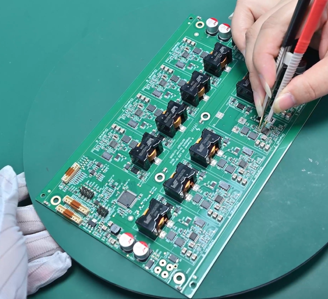
They maintain placement accuracy within ±25 microns, reliably handling 01005-sized components with a component loss rate controlled below 50 parts per million (PPM). Meanwhile, high-precision multifunctional machines handle complex and high-precision components like BGAs, QFPs, connectors, and sensors, achieving placement accuracy within ±15 microns.
For fine-pitch chips (pin pitch <0.3mm), positional deviation is kept within one-tenth of the pin width, preventing issues like cold joints or solder bridging caused by pin misalignment at the source. Experienced manufacturers also customize component feeders and vacuum nozzles for specific products and optimize placement programs for unique components—such as irregularly shaped sensors or ultra-thin FPC boards—further boosting placement yields to over 99.99%.
The core of the soldering process is the nitrogen-atmosphere reflow oven with ten or more heating zones. AI smart terminal motherboards contain a mix of components with varying thermal tolerances, ranging from high-temperature-resistant metal-packaged chips to heat-sensitive plastic-packaged sensors and flexible circuit boards. Improper reflow temperature profiles can easily lead to component damage from excessive local heat or “cold joints” caused by insufficient heat preventing proper solder melting.
Utilizing a nitrogen atmosphere significantly reduces solder surface oxidation and improves wetting; this ensures the formation of full, glossy, and reliable solder joints—even for the underside pads of 0.3mm fine-pitch BGAs—while drastically reducing void rates. Professional manufacturers test and customize specific reflow temperature profiles for each PCB design, accounting for varying materials and component layouts. By using oven profilers to capture real-time temperature data across the board, they ensure that every component is soldered within the optimal temperature range, avoiding both heat-induced damage and inadequate soldering.
The inspection process must implement a triple-inspection system comprising AOI, X-Ray, and 3D AOI. Following reflow soldering, high-speed, high-definition vision cameras perform a full-angle scan of the entire PCB to automatically identify common soldering defects—such as cold joints, solder bridging, misalignment, tombstoning, and reversed components—achieving 100% inspection coverage and eliminating the risk of missed defects associated with manual visual inspection.
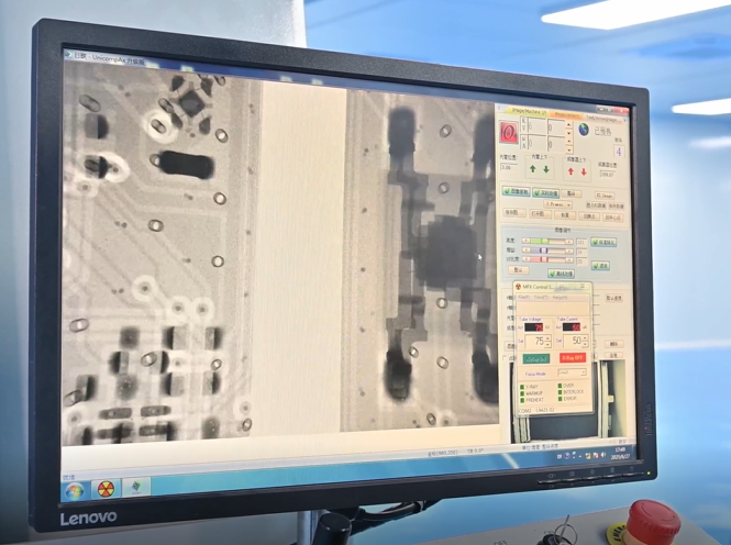
For solder joints (such as those on BGAs) that are obscured by the chip body and inaccessible to top-down optical inspection, X-Ray equipment is used to penetrate the chip casing and directly examine the formation of internal joints, checking for voiding, cracks, and cold joints. To meet requirements for measuring solder joint height and volume, 3D AOI equipment is additionally deployed; 3D scanning precisely captures latent soldering defects that conventional 2D vision systems cannot detect, ensuring that the quality of every solder joint remains under control.
III. The True Technical Barrier: Core Process Expertise That Ordinary Factories Cannot Replicate
If high-end equipment serves as the admission ticket to this sector, then the process technology system—honed through hundreds of projects—constitutes the truly irreplaceable core competitiveness of a PCB assembly manufacturer. Even with identical equipment, the yield, stability, and product reliability achieved by different teams can vary drastically.
Assembly service providers deeply rooted in the fields of AI smart terminals and wearable devices develop specialized process technologies tailored to these products, enabling them to solve complex manufacturing challenges that are beyond the capabilities of most ordinary factories.
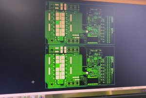
The first core process capability is front-end DFM (Design for Manufacturability) review. Many R&D teams send PCB design files directly to the factory for production, only to discover issues during the SMT (Surface Mount Technology) stage—such as unreasonable pad dimensions, component spacing that is too tight for stencil aperture requirements, or overly dense routing that causes widespread solder bridging. These issues necessitate board redesigns, resulting in significant waste of time and cost. Professional PCB assembly service providers, however, deploy teams of process engineers with over a decade of industry experience to conduct comprehensive, in-depth DFM reviews of client Gerber files and BOMs before production begins.
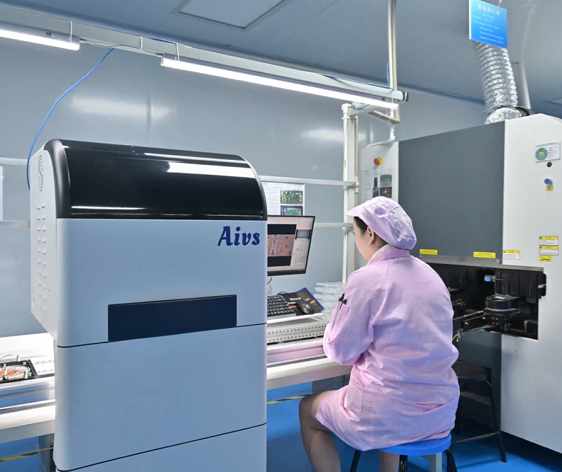
By addressing multiple dimensions—including pad size optimization, component spacing adjustments, stencil aperture design, thermal path planning, and panelization strategies—they identify hidden manufacturing risks early on. Through minor design tweaks that do not alter product functionality or performance, they can boost the “first-pass yield” in subsequent mass production by more than 15 percentage points. This ability to optimize processes at the source is a capability that most ordinary SMT factories lack, yet it represents the precise type of manufacturing-side support that R&D teams need most.
The second core process capability is high-precision placement and rework for 0.3mm fine-pitch BGAs (Ball Grid Arrays). As pin pitches and solder ball diameters on edge AI computing chips shrink, inadequate control over placement and soldering processes can easily lead to issues such as excessive voiding in BGA solder joints, cold solder joints, or chip misalignment after soldering—all of which directly compromise the operational stability of AI computing modules. By optimizing solder paste alloy composition, adjusting reflow soldering ramp rates and soak zone durations, and utilizing a high-purity nitrogen atmosphere, specialized factories can keep the average void ratio of BGA solder joints below 10%—far better than general industry standards.
To address the frequent need for chip rework during the R&D phase, factories are equipped with professional BGA rework stations and high-precision visual alignment systems. These enable the complete process—chip removal, pad cleaning, re-balling, precise placement, and soldering. Reworked chips meet the same reliability standards as newly soldered ones without damaging surrounding 01005-sized micro-components, ensuring R&D teams do not have to scrap an entire high-value motherboard due to a single faulty chip.
The third core process involves anti-deformation support using carriers for ultra-thin, irregularly shaped boards. Ultra-thin PCBs (under 0.3mm thick) are prone to warping and deformation due to uneven thermal stress during high-temperature reflow soldering. If deformation exceeds permissible limits, it can cause component placement misalignment and solder joint fractures.
Experienced process teams create custom, high-temperature-resistant synthetic stone carriers for each specific irregular thin board design. The PCB is securely mounted flat against the carrier, which remains attached throughout the entire workflow—from printing and component placement to reflow soldering. The carrier’s rigidity counteracts the board’s thermal deformation, keeping total board warpage within 0.5% and effectively solving the industry-wide challenge of soldering deformation in thin boards.
For rigid-flex boards, high-temperature-resistant adhesive tape is applied to support flexible areas, preventing wrinkling or shifting during production and ensuring consistent component placement and soldering quality across the entire board.
The fourth core process is impedance consistency control for high-speed signal applications. Motherboards equipped with high-speed AI processors and communication modules impose strict requirements on differential pair impedance precision; impedance values must typically be controlled within ±5% of the design target, with some high-end applications requiring a tolerance of just ±3%. If the amount of solder on the pads is excessive or insufficient during PCB assembly, the impedance of local traces changes, leading to signal reflection and excessive attenuation, which ultimately compromises high-speed signal integrity.
A professional engineering team collaborates with the PCB fabrication plant in advance to ensure the baseline impedance accuracy of the bare board through measures such as optimizing the stack-up structure, adjusting trace widths and spacing, and refining solder mask openings. Subsequently, customized stencil aperture designs are used to strictly control the volume of solder paste on the pads, preventing solder quantity from altering local impedance characteristics. This ensures high-precision impedance consistency across the entire board, enabling the AI chip to reliably perform high-speed computing and communication functions.
The fifth core process involves reliability enhancement for wearable applications. To meet the specific demands of long-term use in wearable products, the factory provides targeted surface coating processes based on the product’s usage scenarios.
Using fully automated selective coating equipment, a transparent protective coating is evenly applied to the tested PCB surface. The process precisely avoids areas that do not require coating, such as sensor contacts and charging terminals. This grants the motherboard resistance against moisture, salt spray, and mold, ensuring that circuits do not corrode even when users wear the device during strenuous, sweat-inducing activities.
For components frequently subjected to vibration and impact—such as connectors and sensors—specialized underfill adhesive is dispensed at the base of the component. Once cured, this adhesive firmly bonds the component to the PCB, significantly enhancing the impact and vibration resistance of the solder joints. Consequently, the product remains intact even after multiple 1.5-meter drop tests, with no risk of component detachment.
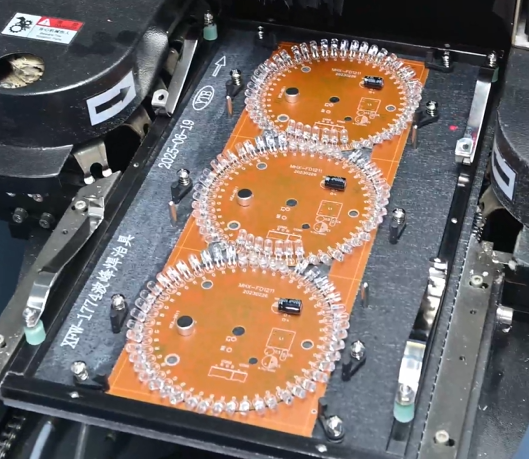
IV. End-to-End Closed-Loop Control: Eliminating Mass Production Risks at the Source
For highly complex products like AI smart terminals and wearable devices, quality control cannot rely solely on final product inspection. Instead, a full-chain, closed-loop control system must be established—spanning from raw material intake to finished product shipment—to intercept quality risks at every process stage. This prevents defective units from proceeding to the next step and, more importantly, averts batch-level quality issues. A truly professional PCB assembly service provider extends quality control measures to every detail of the production process, utilizing standardized protocols and digital systems to ensure the entire workflow is fully controllable and traceable.
Incoming material inspection serves as the first line of defense. For core components—such as chips and sensors used in AI smart terminals and wearable devices—the inclusion of counterfeit, refurbished, or salvaged parts can lead to latent defects in the final product, regardless of how flawless the assembly process might be. Factories implement rigorous Incoming Quality Control (IQC) procedures; upon arrival, components undergo verification of brand, model, batch number, and packaging details. Preliminary screening for substandard materials is conducted through visual inspections, pin coplanarity checks, and verification of silkscreen markings.
For high-value core components like BGA chips and AI processors, X-ray equipment is used to inspect internal packaging quality. This process screens for hidden defects—such as internal cold solder joints or chip cracking—preventing substandard materials from entering the production line. Furthermore, all components are stored in warehouses with controlled temperature and humidity, adhering to strict anti-static protocols. Moisture-sensitive devices (MSDs) are managed according to specific moisture-sensitivity level requirements to prevent moisture absorption during storage, which could otherwise cause internal cracking during soldering.
The Manufacturing Execution System (MES) acts as the core platform for digital management and control. Every PCB entering the production line is assigned a unique traceability identifier. Production data, equipment parameters, and inspection results from every stage—including solder paste printing, SPI, SMT placement, reflow soldering, AOI, X-ray inspection, post-soldering, functional testing, and final packaging—are uploaded to the MES in real-time.
If a defect occurs at any stage, the system instantly records the specific workstation, equipment, operator, and defect type. Should the volume of a particular defect type exceed a preset warning threshold, the system automatically triggers an alert. Process engineers then intervene immediately to analyze the root cause, addressing the issue at the source to prevent batch defects.
Additionally, the system allows customers to check order progress, yield data, and inspection reports at any time, ensuring complete transparency throughout the production process with no information “black boxes.”
A comprehensive anti-static system provides the fundamental safeguard for precision components. Components such as edge AI chips and MEMS sensors used in smart AI devices are highly sensitive to static electricity. Even an electrostatic discharge (ESD) of just a few hundred volts can cause latent internal damage; while products may pass factory inspections and function normally at the time of shipment, they can develop random functional failures after a period of use.
Professional manufacturing facilities establish comprehensive ESD control systems. These range from ESD discharge devices at workshop entrances to anti-static work surfaces, wrist straps, and protective clothing on the production line, as well as reliable grounding for all production equipment. Regular ESD testing is conducted at every stage to ensure that static voltage levels throughout the workshop remain within safe limits.
All personnel handling PCB assemblies must undergo ESD training and pass an assessment before commencing work, thereby eliminating the risk of component damage caused by human handling.
Upfront reliability verification serves as the final checkpoint before mass production. For every new product project, the factory conducts a small-batch pilot run prior to full-scale production, followed by environmental reliability testing on a sample of the finished boards.
Through a series of tests simulating extreme usage scenarios—such as thermal cycling (-40°C to 85°C), high-temperature/high-humidity aging (85°C/85% RH), random vibration, and 1.5-meter drop tests—the reliability of the PCB assembly process is verified. This allows for the early detection of latent issues such as insufficient solder joint strength, insecure component mounting, or poor thermal stress matching, enabling process optimizations to be made before mass production begins.
Many factories also implement a 72-hour (or longer) system-level aging test process. All finished boards undergo continuous operation while powered on to simulate long-term user activity. This ensures that any units prone to early-life failure are intercepted within the factory, guaranteeing that every board delivered to the customer has undergone rigorous reliability verification. ## V. Full-Chain Localized Collaboration: The Core Manufacturing Advantage of Shenzhen’s AI Hardware Industry
For R&D teams developing AI terminals and wearable devices in Shenzhen, the value of PCB assembly service providers extends far beyond simple SMT (Surface Mount Technology) processing. Instead, it lies in creating a one-stop, full-chain service capability—encompassing rapid PCB prototyping, full-BOM component sourcing, SMT assembly, functional testing, and final product assembly. This allows clients to manage the entire workflow—from prototype development to mass delivery—through a single point of contact.
The seamless integration of rapid PCB fabrication and SMT prototyping significantly shortens the R&D iteration cycle. Many hardware startups in Shenzhen operate at a rapid pace, often requiring design revisions and new, debug-ready prototypes within a single week. Under the traditional model, a client would first commission a PCB factory to produce bare boards; after waiting 3–5 days to receive them, they would then engage an SMT factory for assembly—a process taking well over a week at best.
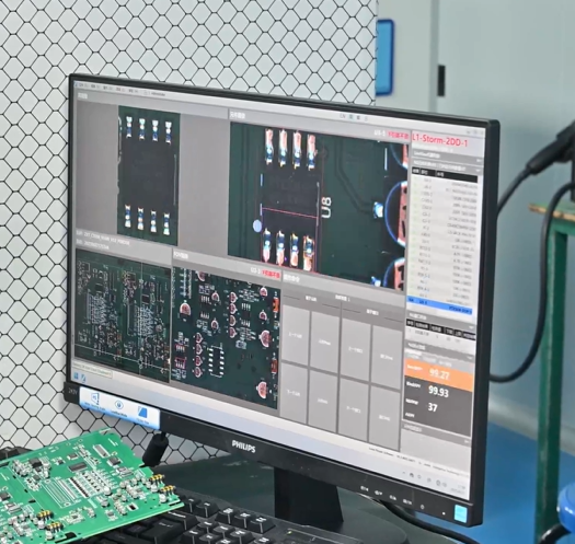
In contrast, service providers with full-chain capabilities can synchronize PCB fabrication and SMT assembly. Once a client uploads Gerber files and the BOM (Bill of Materials), the factory simultaneously initiates PCB production and component sourcing. By the time the bare boards are ready, the components are also on hand, allowing the assembly process to begin immediately. This enables the delivery of assembled prototype boards within as little as 24 hours, allowing R&D teams to receive and debug prototypes on the same day, thereby drastically accelerating product iteration.
Robust full-BOM component sourcing capabilities help clients overcome material procurement challenges. The BOM for an AI smart terminal often includes dozens or even hundreds of different component models. Many emerging sensors and AI chips have limited market supply and fragmented procurement channels; sourcing them individually during the small-batch R&D phase is not only costly but also carries a high risk of purchasing counterfeit parts. An assembly service provider with extensive industry experience establishes long-term, stable partnerships with major global chip manufacturers and Tier-1 distributors. Backed by a supply chain covering a full range of components, they offer one-stop BOM (Bill of Materials) sourcing—rapidly procuring everything from standard passives (resistors, capacitors, inductors) to scarce AI processors and MEMS sensors—while guaranteeing material quality through legitimate channels and preventing the inclusion of counterfeit or refurbished parts. For materials in short supply, the factory leverages its own supply chain resources to coordinate stock, preventing project delays caused by shortages.
The ability to transition smoothly from small-batch R&D runs to large-scale mass production is a critical factor often overlooked by many teams. Products may function perfectly during the prototype stage (producing dozens of units), only to suffer a sharp drop in yield when scaling up to thousands or tens of thousands of units; fundamentally, this occurs because the manufacturing processes devised during R&D failed to account for mass-production compatibility.
Professional assembly service providers integrate mass-production considerations early in the R&D and prototyping phases. When formulating manufacturing processes, they prioritize stability for future large-scale production, avoiding unique, non-replicable “quick-fix” methods used solely for rapid prototyping.
When a product transitions from small-batch validation (dozens of units) to mass production (tens or hundreds of thousands of units), the factory can rapidly replicate mature, stable processes across multiple production lines. By using an MES (Manufacturing Execution System) to centrally manage parameters and standards, they ensure consistent quality across different production batches, preventing quality control issues during mass production.
In an era of rapid technological iteration for AI edge devices and wearables, choosing a PCB assembly service provider with deep technical expertise is not merely selecting a supplier—it is choosing a long-term technical partner.
Such a partner helps you avoid hidden manufacturing pitfalls during R&D, rapidly validates process stability during small-batch pilot runs, and safeguards quality and delivery schedules during mass production. Ultimately, they enable your AI hardware product to transition securely from a technical concept to the market, achieving true commercial success.
About KingTop Technology
As a professional PCB assembly factory in China, KingTop Technology provides one-stop electronic manufacturing services, covering everything from design, high-quality PCB fabrication, precise SMT & DIP assembly to supply chain management, bringing your products to market with speed and precision.