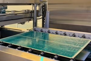
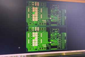
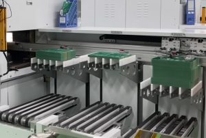
The explosive growth of generative AI, large-scale models, inference, training, and High-Performance Computing (HPC) is fundamentally reshaping server hardware architecture.
Compared to traditional enterprise servers, AI servers demand not only extreme computing power but also set new, comprehensive hardware engineering benchmarks for high-speed signal transmission, high-power delivery, advanced thermal management, mechanical integration, and stability under continuous high-load operation.
In this industrial landscape, the PCB is no longer merely a basic component for “connecting electronic parts”; it has become a core hardware element within the AI server system, directly influencing signal transmission, power distribution, computing performance, and overall system reliability.
Products such as AI server motherboards, GPU accelerator cards, AI accelerator cards, baseboards, switch boards, power boards, and high-speed backplanes typically feature high layer counts, high density, high data rates, high current capacity, and high reliability. These characteristics place stringent demands on the engineering, manufacturing, and quality management capabilities of PCB manufacturers and assemblers.
Consequently, for professional PCB manufacturers and assemblers, producing AI server PCBs involves more than simply making traditional server PCBs “larger, thicker, or with more layers.” It requires establishing a comprehensive, mass-production-ready engineering system covering everything from material selection, stack-up design, impedance control, circuit fabrication, drilling, lamination, plating, and surface finishing to SMT assembly, BGA soldering, X-ray inspection, ICT/FCT testing, and reliability verification.
This article provides an in-depth analysis—from the practical perspectives of PCB manufacturing and assembly—of the technical characteristics, manufacturing challenges, assembly requirements, and key considerations for supplier selection regarding AI server motherboards and AI accelerator card PCBs.
What is an AI Server PCB?
AI server PCBs are high-end printed circuit boards primarily used in AI servers, GPU servers, high-performance computing (HPC) platforms, and data center computing equipment. In terms of system architecture, AI servers typically comprise several key PCB modules, including:
- AI server motherboard
- GPU accelerator card PCB
- AI accelerator card
- GPU baseboard
- CPU compute board
- High-speed switch board
- PCIe expansion card
- NIC (Network Interface Card)
- Power management board
- Backplane
- Storage board
- Fan control board
- Power distribution board
Among these, the motherboard and the AI accelerator card are generally the components with the most demanding PCB technical requirements.
The AI server motherboard is responsible for high-speed data exchange between the CPU, memory, GPU, PCIe interfaces, high-speed networking, storage devices, and various management/control circuits; consequently, it faces simultaneous challenges regarding high-speed signal integrity and high-power power integrity.
GPU accelerator cards and AI accelerator cards typically connect directly to high-performance GPUs, AI ASICs, HBM interfaces, and high-speed PCIe or other high-speed SerDes interfaces. As a result, they impose even stricter requirements regarding high-speed signal transmission, power distribution, thermal management, and board-level reliability.
How do AI server motherboard PCBs differ from standard server PCBs?
While traditional server motherboards are already considered high-end PCB products, AI servers have further elevated the technical requirements for PCBs.
The first significant difference is the substantial increase in high-speed signal transmission density.
Modern AI servers must handle GPUs, CPUs, HBM, DDR memory, PCIe, Ethernet, InfiniBand, and other high-speed interconnect architectures. As data transmission rates continue to rise, PCB routing is no longer merely a matter of establishing electrical continuity; it requires precise control over transmission loss, impedance, crosstalk, reflections, and timing.
The second difference is power density.
The power consumption of AI GPUs and AI accelerators far exceeds that of traditional general-purpose computing platforms. When a single system is configured with multiple high-power GPUs or AI accelerator cards, the motherboard and accelerator cards must handle extremely high current delivery demands.
This necessitates superior designs for power planes, copper thickness control, via structures, current-carrying capacity, and thermal management capabilities.
The third difference lies in mechanical and thermal reliability.
AI servers often operate under high loads for extended periods; therefore, the PCBs must maintain stable performance under conditions of high temperatures, high currents, and frequent thermal cycling. Therefore, material selection, lamination structure, CTE control, solder joint reliability, and the control of board warpage are all critical factors for PCBs.
Core Manufacturing Technologies for AI Server Motherboard PCBs
High-Layer-Count PCB Manufacturing Capabilities
AI server motherboards typically require numerous power planes, ground planes, and high-speed signal layers, resulting in a high layer count.
The true challenge of high-layer-count PCBs lies not merely in the number of layers, but in maintaining dimensional stability and interlayer registration accuracy after lamination.
Dimensional tolerances accumulate throughout the manufacturing process—including inner-layer exposure, etching, brown oxide treatment, lay-up, lamination, drilling, and subsequent plating.
As the layer count and board thickness increase, even minute deviations in any single process step can be amplified in the final product.
Consequently, manufacturers of high-end AI server PCBs must possess mature high-layer-count processing capabilities, alongside comprehensive engineering compensation and process control expertise.
Application of HDI and High-Density Interconnect Technology in AI Accelerator Cards
AI accelerator cards require the routing of numerous high-speed signals and the placement of high-density BGA components within a limited PCB footprint; thus, HDI technology plays a vital role in certain high-end products.
HDI PCBs enhance routing efficiency through the use of microvias, blind vias, buried vias, and higher-density circuit structures.
For instance, GPUs or AI ASICs are typically paired with high-pin-count BGA packages. As BGA pitches shrink, traditional through-hole vias may consume excessive routing space.
HDI structures and microvias improve “escape routing” capabilities, allowing high-speed signals and power networks to be routed out of the chip package area more efficiently.
However, more HDI layers do not necessarily equate to a better design.
PCB manufacturers must select an appropriate HDI structure based on factors such as high-speed signal requirements, power design, board thickness, cost, reliability, and mass production capabilities.
For AI server PCBs, the priority is “manufacturable HDI” rather than the pursuit of extreme line widths/spacings or overly complex microvia structures.
Material Requirements for High-Speed AI Server PCBs
High-speed PCB materials are a critical aspect of the design and manufacturing of AI server PCBs.
As signal transmission rates increase, the dielectric constant (Dk), dissipation factor (Df), dielectric loss, and frequency characteristics of the PCB dielectric material directly impact high-speed signal quality.
While standard FR-4 materials meet the needs of many traditional electronic products, specific high-speed AI server applications require low-loss or ultra-low-loss materials.
Common material selection categories include:
- Low-loss materials
- Mid-loss materials
- Low-Dk materials
- Low-Df materials
- High-Tg materials
- Materials with high dimensional stability
- High heat-resistance materials
- High-frequency, high-speed copper-clad laminates (CCL)
Material selection cannot be based solely on the material’s Dk or Df values.
PCB manufacturers must also consider factors such as actual post-lamination thickness, resin content, copper foil roughness, lamination conditions, the coefficient of thermal expansion (CTE), and batch-to-batch consistency.
For high-speed AI server PCBs, materials, the layer stack-up, and the manufacturing process must be considered holistically.
Stack-up Design: Key to Successful Mass Production of AI Server PCBs
Designing the stack-up for an AI server PCB involves more than simply arranging signal, power, and ground layers in sequence.
A robust stack-up design requires simultaneous consideration of:
- High-speed signal impedance
- Power integrity (PI)
- Signal integrity (SI)
- Inter-layer spacing
- Copper thickness
- Dielectric thickness
- Total PCB thickness
- Via structure
- Thermal conductivity
- Lamination reliability
- PCB warpage
- Manufacturing tolerances
For instance, high-speed differential signals require a stable reference plane layer to minimize discontinuities in the return path.
Inconsistent dielectric thickness between the high-speed signal layer and the reference plane can lead to impedance deviations.
Therefore, before commencing mass production, PCB manufacturers must conduct Design for Manufacturability (DFM) analysis on the engineering data provided by the customer (e.g., Gerber, ODB++, or IPC-2581 files).
When necessary, they must also collaborate with the customer’s PCB layout engineers and SI/PI engineers to finalize the stack-up design.
Impedance Control: A Core Capability in AI Server PCB Manufacturing
High-speed server PCBs typically involve extensive controlled impedance requirements. Common structures include:
- Differential Impedance
- Single-ended Impedance
- Microstrip
- Stripline
- Embedded Stripline
Impedance control for high-speed signals cannot rely solely on theoretical values derived from design software.
During actual PCB fabrication, factors such as trace width, trace spacing, copper thickness, dielectric thickness, material dielectric constant (Dk), etching undercut, and lamination thickness all influence the final impedance.
Consequently, established PCB manufacturers design impedance test coupons during the engineering phase and conduct actual measurements using equipment such as TDR (Time-Domain Reflectometry).
This is also why quotes for high-end AI server PCBs cannot be simply compared with those for standard PCBs.
The true cost encompasses more than just materials; it includes material control, engineering validation, impedance testing, manufacturing capabilities, and quality traceability.
Why are AI accelerator card PCBs particularly difficult to manufacture?
AI accelerator card PCBs are typically critical, high-end components within AI servers.
The primary challenges lie in four areas:
First, high speed.
Second, high current.
Third, high-density BGA (Ball Grid Array).
Fourth, high thermal load.
GPUs and AI accelerators typically feature a large number of high-speed I/O and power pins, requiring extensive routing within a very limited PCB area.
Simultaneously, the VRM (Voltage Regulator Module) on the accelerator card must deliver stable, high-current power.
Poor design of the PCB power planes can lead to IR drop, power noise, or localized overheating.
Furthermore, as accelerator cards operate under high loads for extended periods, the PCB and solder joints must withstand continuous thermal cycling.
Therefore, the design and manufacturing of accelerator card PCBs must treat high-speed performance, power delivery, and thermal reliability as an integrated whole.
High-current PCB manufacturing: Copper thickness and power plane design
A significant trend in AI servers is the continuous increase in power consumption.
As current levels rise, the design of the PCB power planes becomes increasingly critical.
A PCB’s current-carrying capacity is directly related to copper thickness, trace width, temperature rise, and heat dissipation conditions.
In high-current applications, manufacturers may need to utilize thicker copper foil, “Heavy Copper” structures, or parallel power planes to distribute the current.
However, PCBs with thick copper layers also present their own manufacturing challenges. For example:
- Etching uniformity
- Line width control
- Copper thickness tolerance
- Plating uniformity
- Interlayer lamination
- Drilling difficulty
- Thermal stress
- Board surface flatness
Therefore, a high-current PCB involves more than simply making the copper thicker.
PCB manufacturers must establish appropriate process solutions based on specific current requirements and structural design.
Drilling and Via Processes for AI Server PCBs
Vias are critical structures in high-end server PCBs.
While traditional through-hole vias involve mature processes, they can restrict routing space in high-density BGA areas.
Consequently, high-end AI PCBs may utilize:
- Through vias
- Blind vias
- Buried vias
- Microvias
- Stacked microvias
- Staggered microvias
- Via-in-pad structures
Among these, the via-in-pad structure demands particularly high manufacturing capabilities.
When a via is placed directly within a BGA pad, processes such as via filling and planarization are typically required to prevent solder paste loss or solder joint defects during the soldering process.
For PCB assembly facilities, the quality of the via-in-pad structure directly impacts BGA solder joint reliability.
Therefore, PCB manufacturing and assembly cannot be considered in isolation.
A PCB design that is feasible to manufacture as a bare board may still encounter issues during mass production if downstream SMT and BGA assembly requirements are not taken into account.
Importance of the Lamination Process for High-Layer-Count AI Server Boards
Lamination is a highly critical process for high-layer-count PCBs.
During the lamination of multilayer boards, the following parameters must be controlled:
- Lamination temperature
- Lamination pressure
- Temperature ramp-up profile
- Dwell time (holding time)
- Resin flow
- Material thickness
- Inter-layer registration
- Board thickness
- Internal stress
AI server motherboards are typically large, feature high layer counts, and possess complex copper distribution; consequently, they are more prone to issues such as warping, bowing, localized resin starvation, and inter-layer misalignment.
This is particularly true when the PCB incorporates both extensive copper planes and high-speed signal layers, as uneven copper distribution between inner and outer layers increases post-lamination stress.
Therefore, PCB manufacturers must evaluate copper balance during the engineering design phase.
AI Server PCB Assembly: SMT Is No Longer Just Simple Component Placement
For AI server PCBs, assembly is a crucial link in the overall supply chain.
High-end server boards typically incorporate CPUs, GPUs, ASICs, BGAs, QFNs, power modules, connectors, and high-speed components, alongside a vast number of passive components. Among these, large-format BGAs, fine-pitch BGAs, and high-density components place extremely high demands on the SMT process.
PCB assembly manufacturers must control the entire process, starting with solder paste printing.
Key processes include:
- SMT solder paste printing
- SPI (Solder Paste Inspection)
- High-precision, high-speed component placement
- Reflow soldering
- AOI (Automated Optical Inspection)
- X-ray inspection
- BGA solder joint analysis
- Manual touch-up/rework
- ICT (In-Circuit Testing)
- FCT (Functional Testing)
- Burn-in or high-load testing
- Final quality inspection
The focus of high-end AI server PCB assembly lies in establishing a stable, traceable, and repeatable process.
BGA Soldering: A Key Focus in AI Server PCB Assembly
AI server motherboards and AI accelerator cards typically utilize a large number of BGA packages.
One of the major challenges with BGAs is that solder joints are located beneath the component, making it impossible to perform visual inspections directly from the PCB surface, unlike with standard SMD components.
Consequently, X-ray inspection is a crucial quality control measure in high-end server PCB assembly.
X-ray inspection allows for the detection of:
- Voids
- Opens
- Shorts
- Solder bridges
- Insufficient solder
- Missing balls
- BGA solder joint anomalies
Additionally, the reflow soldering profile is critical.
Factors such as PCB material, PCB thickness, BGA components, and component thermal mass can all influence the actual temperature profile.
Therefore, SMT engineers must establish an appropriate profile based on the specific product, rather than simply using fixed reflow parameters.
SPI, AOI, and X-ray Inspection in AI Server PCB Assembly
For high-end AI server products, no single inspection tool can cover every potential quality issue.
SPI is primarily used to inspect solder paste printing quality, checking parameters such as solder paste volume, height, area, and offset.
AOI is mainly used to check component placement, polarity, solder joint appearance, and soldering defects in visible areas.
X-ray inspection is suitable for examining BGAs, QFNs, and other solder joints that are not directly visible.
Combining these three methods enables more comprehensive SMT quality control. Furthermore, for high-reliability AI server PCBs, manufacturers must establish a comprehensive process traceability system, covering:
- PCB Lot
- Component Lot
- Solder Paste Lot
- SMT Machine Data
- Reflow Profile
- SPI Data
- AOI Data
- X-Ray Data
- Operator Record
- Repair Record
- Testing Record
This data is crucial for subsequent quality analysis and customer audits.
The Importance of PCB Surface Finish for AI Server Products
The surface finish for high-end server PCBs is typically selected based on product structure and assembly requirements.
Common methods include:
- ENIG
- ENEPIG
- OSP
- Immersion Tin
- Immersion Silver
- HASL, etc.
Surface flatness and solder joint reliability are critical for fine-pitch BGAs, high-density SMT, and high-reliability applications.
For instance, ENIG offers superior surface flatness, making it suitable for certain products featuring high-density layouts and fine-pitch pads.
If a product involves high-frequency/high-speed signals, fine-pitch BGAs, and high-reliability requirements, PCB manufacturers must conduct a comprehensive evaluation considering factors such as solderability, surface flatness, gold layer structure, reliability, and cost.
PCB Warpage and Bowing: Critical Issues to Control in AI Server Mass Production
AI server PCBs are typically large, have high layer counts, and feature thick copper layers; they often accommodate large BGAs and high-power components.
Consequently, board bowing and warpage directly impact SMT assembly quality.
Excessive PCB warpage can lead to:
- Uneven solder paste printing
- Component placement misalignment
- BGA soldering defects
- Open circuits
- Head-in-Pillow defects
- Post-reflow board deformation
- Connector mating issues
Therefore, material symmetry, copper foil distribution, lamination structure, and thermal stress must be controlled during the PCB fabrication stage.
During the PCB assembly stage, controls must be implemented regarding SMT equipment, fixtures, and reflow soldering conditions.
This underscores the necessity of adopting an integrated “PCB Fabrication + PCB Assembly” approach for high-end AI server PCBs.
Thermal Management for AI Server PCBs
Heat dissipation is one of the most critical challenges for AI servers.
Components such as GPUs, CPUs, AI accelerators, and VRMs generate significant heat; the PCB serves not only to provide electrical connections but also plays a role in heat conduction.
Thermal management can be improved through measures such as increasing copper thickness, designing large copper planes, utilizing thermal vias and via arrays, and implementing optimized power/ground structures.
For high-power BGA components, a large number of thermal vias may need to be designed on the underside of the PCB to facilitate heat transfer to internal layers or heat dissipation structures.
However, the number and placement of thermal vias must also take into account manufacturing capabilities and reliability.
Therefore, thermal design should not be the sole responsibility of mechanical engineers; instead, it requires the collaborative participation of PCB layout designers, PCB manufacturers, SMT assembly teams, and thermal engineers.
Power Integrity (PI) Requirements for AI Server PCBs
In high-power AI servers, power integrity has become a crucial aspect of PCB design.
Current demands from GPUs and CPUs fluctuate rapidly depending on the computational load.
A poorly designed Power Distribution Network (PDN) can lead to issues such as:
- Voltage drop
- Power noise
- Ground bounce
- EMI
- Local heating
- Power instability
Consequently, AI server PCBs require optimized power planes, decoupling capacitors, via arrays, and power return paths to minimize power impedance.
PCB manufacturers must ensure that the actual manufactured dielectric thickness, copper thickness, and circuit structures comply with the design specifications.
For high-end PCBs, minimizing the discrepancy between design data and actual manufacturing results leads to greater system performance stability.
Signal Integrity (SI) Requirements for AI Server PCBs
Signal integrity is equally critical in high-speed AI server PCBs.
High-speed signals can encounter issues due to factors such as:
- Impedance mismatch
- Via stubs
- Trace discontinuities
- Crosstalk
- Insertion loss
- Return loss
- Reflection
- Material loss
- Connector discontinuities
Therefore, PCB layout engineers must conduct SI analysis during the design phase, while PCB manufacturers need to translate these design requirements into manufacturing specifications suitable for mass production. For example:
“100Ω Differential Impedance” is not merely a single figure for a PCB manufacturer to control; it must be translated into specific parameters such as trace width, trace spacing, dielectric thickness, copper thickness, material dielectric constant (Dk), and manufacturing tolerances.
Therefore, a supplier truly capable of handling high-end server PCBs must possess integrated capabilities in DFM (Design for Manufacturability) and SI/PI (Signal Integrity/Power Integrity).
What capabilities must PCB manufacturers possess for AI server products?
When seeking a supplier for AI server PCBs, companies should not focus solely on the unit price of the PCB.
It is more important to determine whether the supplier possesses the following capabilities:
Mass production capability for high-layer-count PCBs
The ability to stably manufacture high-layer, multi-layer, and thick PCBs, rather than relying merely on the capacity to produce small batches of samples.
Experience with high-speed materials
Familiarity with the lamination and processing characteristics of Low Loss, Low Df, and high-Tg materials.
Impedance control capability
Proficiency in impedance calculation, test coupon design, TDR testing, and process control.
High-density BGA capability
Experience with Fine Pitch BGA, Via-in-Pad, Microvia, and HDI manufacturing.
High-current PCB capability
The ability to handle thicker copper foil, high-current power layers, and large-area copper planes.
Dimensional stability control
The ability to control board thickness, dimensions, and warpage for high-layer-count, large-format PCBs.
Comprehensive quality management
Including AOI (Automated Optical Inspection), X-ray inspection, electrical testing, impedance testing, cross-section analysis, and reliability testing.
What SMT capabilities for AI servers must PCB assembly manufacturers possess?
Beyond the fabrication of bare PCBs, AI server PCB assembly also requires specialized process capabilities.
First is high-precision SMT equipment.
Second is stable solder paste printing capability.
Third is the capability to place BGA and fine-pitch components.
Simultaneously, robust reflow profile management is required.
For large BGAs and high-value AI components, X-ray inspection is an essential process that cannot be overlooked. In addition, certain AI server products may require the following:
- ICT (In-Circuit Testing)
- FCT (Functional Circuit Testing)
- Boundary Scan
- Firmware Programming
- Functional Testing
- Burn-in
- Thermal Testing
- High-Load Testing
These tests help mitigate the risk of system failures caused by soldering, component, or circuitry issues prior to product shipment.
Why is a one-stop supply chain needed for the transition from PCB fabrication to PCB assembly?
For AI server clients, having different suppliers handle PCB fabrication and PCB assembly separately can easily lead to gaps in engineering information.
For instance, a PCB manufacturer might focus solely on bare board dimensions, whereas an SMT factory focuses on soldering.
However, AI server PCBs require a holistic view of the product.
For example: Is “Via-in-Pad” suitable for BGA soldering?
Does the PCB thickness affect the reflow soldering process?
Does the copper thickness cause variations in reflow thermal capacity?
Will PCB warpage affect the soldering of large BGAs?
Is the surface finish suitable for fine-pitch components?
These issues require collaborative consideration by both the PCB fabrication and assembly teams.
Therefore, a supplier offering one-stop services—covering both PCB fabrication and assembly—can facilitate more efficient engineering communication, problem analysis, and quality traceability.
Quality management in AI server PCB fabrication
AI servers are typically deployed in data centers, cloud computing platforms, enterprise-grade AI systems, and high-performance computing (HPC) environments.
These products often require continuous, long-term operation.
Consequently, PCB quality assurance cannot rely solely on final inspection; a comprehensive process quality management system must be established.
Examples include:
IQC (Incoming Quality Control)
Verifying that PCB materials, copper-clad laminates (CCL), prepreg (PP), copper foil, and other raw materials meet specifications.
IPQC (In-Process Quality Control)
Monitoring quality during processes such as inner-layer fabrication, lamination, drilling, plating, circuit patterning, solder mask application, and surface finishing.
FQC (Final Quality Control)
Verifying dimensions, appearance, electrical properties, impedance, and other specifications of the finished product.
OQC (Outgoing Quality Control)
Verifying the final product for shipment, including packaging, quantity, labeling, and traceability data.
For high-end AI server products, a comprehensive quality system is far more critical than a single final inspection.
Reliability testing for AI server PCBs
High-end PCB products typically require reliability validation based on customer specifications and product applications. Common tests include:
- Thermal Stress
- Thermal Cycling
- High Temperature Storage
- Humidity Test
- Solderability Test
- CAF Test
- IST
- PCT
- HAST
- Cross-sectioning
- Peel Strength
- Plating Thickness
- Microsection Analysis
Among these, CAF (Conductive Anodic Filament) formation is a particular concern for high-layer-count, high-density PCBs.
As PCB circuit density increases and the spacing between layers decreases, the reliability requirements for materials and manufacturing processes also rise.
Consequently, PCB manufacturers must mitigate associated risks through careful material selection, control of drilling quality, rigorous cleaning processes, and effective lamination management.
DFM Considerations in AI Server PCB Manufacturing
Many PCB issues do not originate during mass production; rather, the risks are often embedded during the layout stage.
Therefore, professional PCB manufacturers should conduct DFM (Design for Manufacturability) analysis prior to prototyping.
DFM analysis primarily covers:
- Line Width
- Line Spacing
- Hole Size
- Annular Ring
- Copper-to-Edge Clearance
- BGA Pad
- Via-in-Pad
- Stack-up
- Impedance
- Copper Balance
- Drill Aspect Ratio
- Surface Finish
- Board Thickness
- Panelization
Identifying issues early through DFM helps reduce the need for subsequent engineering changes and minimizes defects during mass production.
DFM is particularly critical for high-value, highly complex products such as AI server PCBs.
How do AI server PCB manufacturers control mass production costs?
High-end PCBs do not necessarily mean pursuing only the highest specifications.
True engineering maturity lies in establishing a rational manufacturing solution that meets electrical performance, reliability, and customer specifications.
For example:
- Unnecessary HDI layer counts can be optimized.
- Overly strict trace width and spacing requirements can be adjusted based on actual needs.
- Unnecessary special materials can be re-evaluated.
- Certain via structures can be simplified.
- Manufacturing costs can be reduced through engineering optimization of the stack-up.
- Material utilization can be improved through panelization.
- In terms of PCB assembly, first-pass yield can be improved by optimizing component coplanarity, solder paste design, stencil design, and SMT programming.
Therefore, cost control for AI server PCBs is not about lowering quality, but about reducing unnecessary manufacturing complexity through engineering expertise.
Future technical trends for AI server PCBs
As the scale of AI models continues to grow, the computing density and power consumption of AI servers are likely to keep rising.
This will further drive PCB development in the following directions:
Higher layer counts
More signal and power layers are needed to support high-speed computing systems.
Lower-loss materials
As high-speed SerDes rates increase, controlling transmission loss in PCB materials becomes increasingly critical.
Higher-density interconnects
Technologies such as HDI, microvias, and via-in-pad will become increasingly important.
Higher current-carrying capacity
As the power consumption of GPUs and AI accelerators rises, PCBs must handle higher currents.
Better thermal management
Co-design between the PCB and the thermal management system will become increasingly important.
Stricter process control
Manufacturing tolerances for AI server PCBs will become tighter.
PCB and package integration
With the development of advanced packaging, high-frequency/high-speed interfaces, and chiplet architectures, electrical and mechanical co-design between the PCB and the IC package will become increasingly important.
Why do AI server PCBs require professional PCB manufacturing and assembly vendors?
AI servers are not ordinary consumer electronics.
A single AI server motherboard may simultaneously involve high-layer-count PCBs, high-speed signals, high currents, high-density BGAs, low-loss materials, strict impedance control, complex thermal management, and high-reliability SMT assembly. Therefore, when selecting a PCB supplier, one should not simply ask, “How many layers can you manufacture?”
Instead, it is crucial to understand:
- Do they have experience with PCBs for AI servers or high-performance computing (HPC)?
- Can they handle high-speed materials?
- Can they provide impedance control?
- Do they possess HDI and microvia manufacturing capabilities?
- Can they handle PCBs with thick copper and high-current requirements?
- Do they have experience with large-scale BGA assembly?
- Do they have SPI, AOI, and X-ray inspection capabilities?
- Can they provide a one-stop service covering both PCB fabrication and PCBA assembly?
- Do they have robust engineering and quality traceability systems?
These factors are what truly determine whether a PCB supplier is suitable for handling high-end AI server products.
The Value of One-Stop Service: PCB Fabrication and Assembly
For AI servers, GPU servers, AI accelerator cards, and HPC equipment, supply chain integration capabilities are becoming increasingly important.
Managing the entire process—from PCB layout data, DFM engineering checks, material selection, stack-up verification, PCB fabrication, and surface finishing to SMT assembly, BGA soldering, AOI, X-ray inspection, and functional testing—within a single supply chain system reduces communication costs across different vendors.
When PCB fabrication and assembly are coordinated by the same team, any BGA soldering issues detected during the SMT stage can be quickly traced back to the PCB fabrication data.
If board warpage is detected, analysis can be conducted on the lamination process and material structure.
If signal anomalies occur during high-speed testing, the issue can be traced back to the stack-up, impedance, materials, and circuit fabrication processes.
This comprehensive capability—extending from bare board fabrication to PCB assembly—is precisely the value required in the high-end AI server PCB supply chain.
Conclusion: Engineering and Mass Production Capabilities Are at the Core of AI Server PCB Competition
The rapid development of the AI server industry is driving a continuous upgrade in the demand for high-end PCBs.
From AI server motherboards to GPU accelerator cards, and from high-speed switch boards to high-power boards, PCBs have become a vital foundation for the entire AI computing hardware architecture. Future AI server PCBs require more than just an increase in layer count; they must simultaneously deliver:
High-speed signal transmission, high-current power delivery, high-density interconnects, low-loss materials, precise impedance control, superior thermal management, and long-term reliability.
Ultimately, these requirements hinge on actual process capabilities in both PCB fabrication and assembly.
PCB manufacturers must possess capabilities in high-layer counts, high-density designs, high-speed materials, HDI, microvias, impedance control, thick copper, and high-reliability processing.
PCB assemblers require capabilities in high-precision SMT, fine-pitch BGA, high-quality solder paste printing, precise reflow, SPI, AOI, X-ray inspection, and comprehensive functional testing.
More importantly, PCB fabrication and assembly can no longer be viewed as two completely separate processes.
From the initial design phase of AI server motherboards and accelerator cards, factors such as DFM (Design for Manufacturability), SI (Signal Integrity), PI (Power Integrity), thermal design, materials, stack-up, fabrication, and assembly must be integrated.
Only through the true integration of design, materials, processes, and testing can high-value, complex products like AI servers balance performance, reliability, mass production efficiency, and cost.
Therefore, for companies seeking AI server PCB suppliers, the true metric for evaluation is not merely the price quote, but whether the supplier possesses comprehensive capabilities—spanning engineering support, fabrication, and assembly—and the ability to consistently translate advanced PCB technology into products suitable for mass production, traceability, and long-term supply.
For AI servers, GPU accelerator cards, AI accelerators, high-performance computing platforms, and data center hardware, the technical threshold for PCBs will only continue to rise.
Consequently, professional PCB fabrication and assembly capabilities will become an indispensable link in the AI hardware supply chain.
About KingTop Technology
As a professional PCB assembly factory in China, KingTop Technology provides one-stop electronic manufacturing services, covering everything from design, high-quality PCB fabrication, precise SMT & DIP assembly to supply chain management, bringing your products to market with speed and precision.