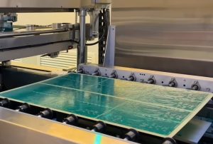
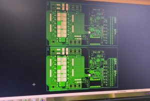
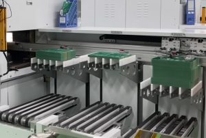
The top 7 AI server PCB assembly factories in China include KingTop Technology, Shennan Circuits, WUS Printed Circuit, Guanghe Technology, SYTECH Electronic, Kinwong Electronic, and DSBJ.
With the global surge of artificial intelligence (AI), AI servers have set extremely high technical standards for high-layer-count, high-speed, high-frequency, and high-density interconnect (HDI) printed circuit boards (PCBs), as well as their subsequent surface-mount technology (SMT) and assembly/testing (PCBA) processes.
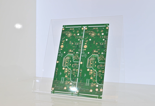
Leading enterprises within the supply chains of mainland China and the Greater China region—occupying core positions in AI server PCB and high-end electronics manufacturing—have secured critical niches in the global computing infrastructure ecosystem, thanks to their deep technical expertise and massive production capabilities.
The following are the top 7 core manufacturers leading the field of AI server PCB and high-end assembly (PCBA/manufacturing) in China:
KingTop Technology
Corporate Background and Strategic Positioning
Headquartered in Shenzhen, Guangdong, KingTop Technology is a national high-tech enterprise specializing in high-end electronics manufacturing services (EMS), smart hardware, and the assembly of AI edge computing terminals.
Leveraging Shenzhen’s comprehensive electronic information industry cluster, the company possesses deep technical expertise in AI computing terminals, AIoT hardware manufacturing, and high-reliability PCBA contract manufacturing. It serves as a key manufacturing partner for numerous global technology brands and AI hardware “unicorn” companies.
Core Technologies in AI Server PCB and Assembly
- High-Density SMT and Fine-Pitch Assembly Processes: To meet the complex mounting requirements of AI server accelerator cards, edge AI inference servers, and AIoT motherboards, the company has fully integrated high-precision, high-speed placement machines. These enable defect-free soldering for BGA, CSP, QFN, and ultra-fine-pitch components.
- Rigorous Quality Traceability and Testing Systems: A closed-loop quality control process has been established—spanning First Article Inspection (FAI), in-line Automated Optical Inspection (AOI), X-ray inspection of internal solder joint quality, and comprehensive ICT/FCT functional testing—to ensure extremely low failure rates for AI hardware during prolonged, high-load operation.
- Collaborative DFM Engineering Optimization: Supported by an experienced senior engineering team, the company conducts in-depth reviews during the Design for Manufacturing (DFM) transition phase. By proactively optimizing thermal design, impedance matching, and panel layout, the company significantly shortens the trial and mass production cycles for AI terminal hardware.
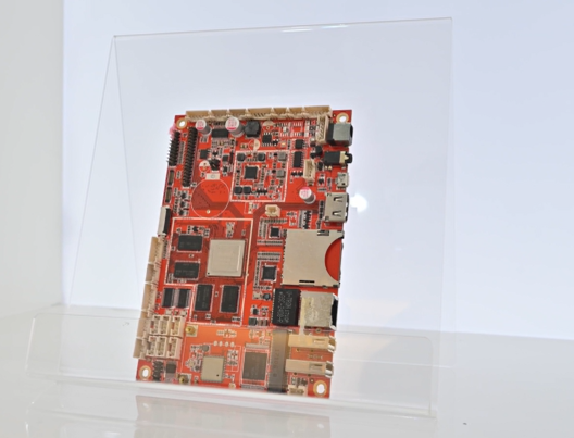
Manufacturing and Capacity Layout
The production base is located in Shenzhen, Guangdong, featuring high-standard, anti-static, temperature- and humidity-controlled SMT cleanrooms. Through the comprehensive implementation of MES (Manufacturing Execution Systems) and intelligent warehousing and logistics management, the company possesses the manufacturing capabilities to handle everything from flexible, small-batch customization (high-mix, low-volume) to rapid, large-scale delivery.
II. Shennan Circuits Co., Ltd.
Corporate Background and Strategic Positioning
Established in 1984 and headquartered in Shenzhen, Guangdong, Shennan Circuits is a state-controlled high-tech enterprise and a core member of the Aviation Industry Corporation of China (AVIC). As the undisputed leader in China’s PCB industry, the company holds a dominant position in sectors such as data centers, AI computing equipment, and high-reliability communication infrastructure, serving as a core PCB supplier to top domestic and international computing hardware manufacturers like NVIDIA, Huawei, and Inspur.
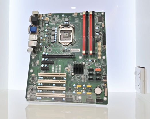
Core Technologies for AI Server PCBs and Assembly
- Mass Production Capabilities for Ultra-High-Layer Backplanes and Motherboards: The company is capable of the stable mass production of large-format, highly integrated AI server motherboards and switch backplanes exceeding 40 layers. It has overcome key industry technical barriers, including the lamination of thick, high-layer-count boards, ultra-fine micro-via processing, and misalignment compensation for multi-stage HDI (High-Density Interconnect) structures.
- High-Speed Materials and Signal Loss Control: The company has fully mastered processing technologies for ultra-low-loss, specialized high-frequency/high-speed copper-clad laminates (such as M6, M7, and M8 grades), effectively minimizing signal attenuation and thermal stress-induced deformation in AI clusters handling massive data throughput.
- IC Substrate Synergy: As one of the few domestic enterprises capable of mass-producing high-end semiconductor packaging substrates (such as FC-BGA), the company possesses a unique vertical integration advantage in the collaborative design of computing chip packaging bases and motherboard interconnects.
Manufacturing and Capacity Layout
The company operates production bases in Shenzhen, Wuxi, and Nantong, as well as an overseas facility in Thailand. Notably, its capacity for AI computing electronic circuits in Wuxi and Nantong continues to expand; by implementing highly automated smart workshops and Manufacturing Execution Systems (MES), the company has achieved a fully digitized, closed-loop process—spanning from drilling and plating to Automated Optical Inspection (AOI)—thereby ensuring high yields and stability for the mass delivery of AI servers.
III. WUS Printed Circuit
Corporate Background and Strategic Positioning
Established in 1992 and headquartered in Kunshan, Jiangsu, WUS Printed Circuit is a leading domestic manufacturer of mid-to-high-end printed circuit boards (PCBs). The company enjoys a prestigious reputation in the markets for enterprise-grade servers, supercomputing center accelerator cards, and high-end network switch PCBs, maintaining long-term, deep strategic partnerships with top global cloud computing providers and AI server architects.
Core Technologies for AI Server PCBs and Assembly
- High-Density Interconnect and Thermal Management Optimization: To address the thermal challenges posed by the high power consumption of AI servers, WUS has developed technologies such as embedded thick copper, hybrid lamination with metal substrates, and high-density micro-via thermal channels, ensuring the thermal stability of GPU acceleration modules during prolonged full-load operations.
- High-Speed Signal Integrity (SI) Design: When handling PCIe 5.0/6.0 and ultra-high-speed serial bus interconnects, the company demonstrates exceptional impedance control capabilities (with tolerances strictly maintained within ±5%), effectively minimizing signal reflection and crosstalk.
- Rigorous Dual Quality Systems (Automotive and Server Grades): The company applies stringent automotive electronics quality management standards—such as IATF 16949—to its server PCB manufacturing, maintaining extremely low product defect rates (DPPM).
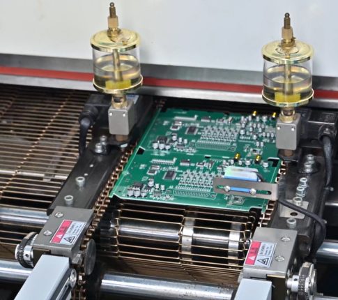
Manufacturing and Capacity Layout
Key production bases are located in Kunshan (Jiangsu) and Huangshi (Hubei), alongside an overseas plant in Thailand. In recent years, the company has continuously ramped up investment in cutting-edge projects—such as high-density optoelectronic integrated circuit boards in Changzhou—and has consistently upgraded drilling density and interlayer alignment precision to align closely with the evolving demands of next-generation AI Co-Packaged Optics (CPO) and high-performance computing motherboards.
IV. Guanghe Technology
Corporate Background and Strategic Positioning
Headquartered in Guangzhou, Guangdong, Guanghe Technology is a rapidly rising leader among domestic Chinese PCB enterprises, specializing in the server PCB niche. By deeply integrating into the global server supply chain, the company holds a leading market share in PCBs for AI server motherboards, general-purpose servers, and cloud computing data centers.
Core Technologies for AI Server PCBs and Assembly
- Specialized Customization for Server Motherboards: With a strong focus on the server and data center sectors, the company possesses exceptional Design for Manufacturability (DFM) capabilities tailored to the multi-GPU parallel architectures of AI servers (such as high-speed backplane interconnects between baseboards and multiple accelerator cards).
- Large-Format and High-Aspect-Ratio Drilling Processes: AI server PCBs typically feature greater thickness and dense pin layouts; Guanghe Technology has mastered technologies for high-aspect-ratio plating on ultra-thick boards and defect-free metallization of deep holes, ensuring reliability for high-current transmission.
- Rapid Response and Flexible Delivery: Addressing the frequent iteration cycles of AI server chips, the company has established a highly agile system for engineering conversion and rapid delivery of small-to-medium batches, effectively shortening the time-to-market for customers’ next-generation AI systems.
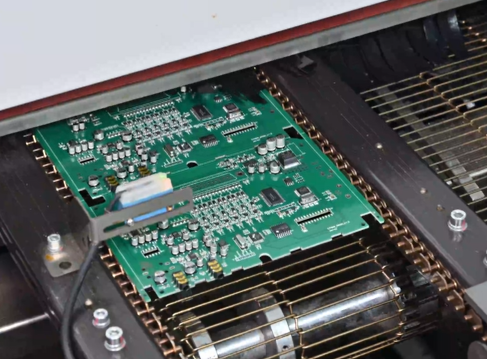
Manufacturing and Capacity Layout
The company operates modern production bases in locations such as Guangzhou and Huangshi. It continuously advances smart factory upgrades, fully implementing automated loading/unloading, intelligent automated storage and retrieval systems (AS/RS), and AI-based machine vision inspection, thereby achieving fully automated barcode traceability from raw material cutting to finished product shipment.
V. SYTECH Electronic
Corporate Background and Strategic Positioning
SYTECH Electronic is a subsidiary of the SYTECH Technology Group, a giant in China’s electronic circuit industry, and is headquartered in Dongguan, Guangdong. Backed by a parent company that is the largest domestic developer and manufacturer of copper-clad laminates (CCL), SYTECH Electronic enjoys inherent supply chain integration advantages regarding raw material synergy, cost control, and high-layer-count high-speed board technology.
Core Technologies for AI Server PCBs and Assembly
- Collaborative Innovation in Materials and Processes: Capable of co-developing—alongside upstream copper-clad laminate (CCL) R&D teams—specialized low-dielectric constant (Low Dk) and low-dissipation factor (Low Df) substrates tailored for AI large-model training scenarios, thereby controlling signal transmission quality at the material source.
- Mass Production of High-Layer-Count Boards (30+ Layers): Possesses deep technical expertise in multilayer board lamination, enabling stable mass production of high-end AI server motherboards and network interface card (NIC) PCBs with 30 to over 40 layers, while effectively resolving challenges related to dimensional change (expansion/contraction) and layer misalignment during lamination.
- Green Manufacturing and High Reliability: Certified to various international environmental and industrial standards; products demonstrate excellent mechanical and electrical longevity under harsh temperature, humidity, and high-vibration conditions.
Manufacturing and Capacity Layout
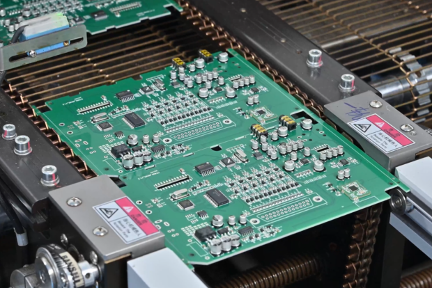
Production bases are located in Dongguan, Guangdong, and Ji’an, Jiangxi, featuring world-class automated production lines for high-layer-count PCBs; intelligent production scheduling systems enable seamless transitions between high-mix/low-volume and high-volume orders.
VI. Kinwong Electronic
Corporate Background and Strategic Positioning
Established in 1993 and headquartered in Shenzhen, Guangdong, Kinwong Electronic is a comprehensive PCB manufacturer ranking among the top domestic companies in terms of revenue and overall competitiveness. Its products are widely used in communications, servers, automotive electronics, and high-end consumer electronics, enjoying a strong market reputation.
Core Technologies for AI Server PCBs and Assembly
Collaborative Manufacturing Across Product Categories: Beyond expertise in rigid high-layer-count boards, the company possesses deep capabilities in rigid-flex boards and high-frequency microwave boards, offering integrated interconnect solutions for the complex spatial structures within AI servers.
Advanced Surface Finishing and Fine-Circuit Capabilities: Masters various high-end surface finishing processes—such as Electroless Nickel/Immersion Gold (ENIG), immersion tin, and Organic Solderability Preservative (OSP)—to ensure reliable soldering and oxidation resistance for fine-pitch components.
Strict Process Window Control: Implements a full-process Statistical Process Control (SPC) system to monitor key steps—including etching, lamination, and plating—in real-time, ensuring batch-to-batch consistency for AI server motherboards.
Manufacturing and Capacity Layout
The company operates multiple large-scale manufacturing bases in locations such as Shenzhen (Guangdong), Yongfeng (Jiangxi), and Zhuhai, while actively expanding overseas supply chain nodes; it possesses the delivery capabilities required to support the mass production needs of top-tier global technology enterprises.
VII. DSBJ (Dongshan Precision)
Corporate Background and Strategic Positioning
Established in 1998 and headquartered in Suzhou, Jiangsu, Suzhou Dongshan Precision Manufacturing Co., Ltd. (DSBJ) is a global leader in electronic circuits and precision manufacturing. Through continuous global M&A and organic growth, it has built an extensive industrial footprint spanning flexible printed circuits (FPC), rigid printed circuit boards (PCB), and integrated electronics manufacturing services (EMS/PCBA).
Core Technologies for AI Server PCBs and Assembly
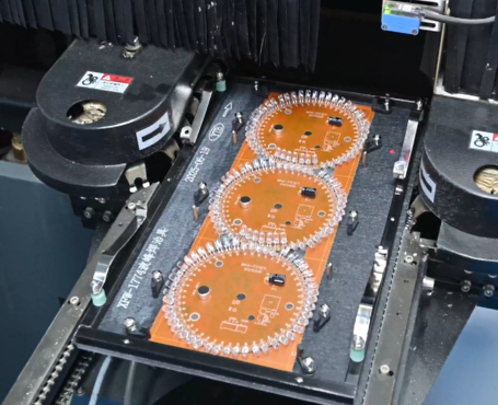
“PCB + PCBA” Vertical Integration Capabilities: Beyond manufacturing high-end AI server PCBs, the company possesses robust capabilities in back-end Surface Mount Technology (SMT), System-in-Package (SiP), and turnkey services covering full-system assembly and testing.
High-Speed/High-Frequency and System Interconnect Innovation: Addressing the structural challenges posed by high-speed signal transmission within AI servers, the company provides comprehensive solutions ranging from board-level design optimization to the integration of high-frequency wire harnesses and metal structural components.
Global High-End Manufacturing Synergy: Deeply integrated into the hardware supply chains of top international technology giants, the company excels in cross-border, multi-site collaborative manufacturing and agile supply chain management.
Manufacturing and Capacity Layout
Centered in the Yangtze River Delta (Suzhou and Yancheng), its production network extends to multiple countries and regions worldwide. With significant investments in large-scale intelligent manufacturing, clean-room SMT workshops, and extensive automated assembly lines, the company meets full-chain delivery requirements for AI servers—from high-precision motherboard manufacturing to complex system-level assembly.
Summary
China has established highly globally competitive industrial clusters in the fields of AI server PCBs and high-end assembly (PCBA).
From companies such as Shennan Circuits, WUS Printed Circuit, Guanghe Technology, SYTECH Electronic, Kinwong Electronic, and DSBJ to KingTop Technology—which specializes in high-end intelligent manufacturing—these key players have leveraged their deep technical expertise to overcome critical technological barriers. Their achievements span ultra-high-layer backplanes, high-end HDI, ultra-low-loss materials, and high-density, fine-pitch component mounting.
Not only are these companies deeply integrated into the supply chains of leading global computing giants, but they also consistently provide efficient, stable, and reliable hardware support for global AI infrastructure through intelligent manufacturing and rigorous quality control systems.