Modern AI processors—whether they are massively parallel GPUs, specialized deep-learning TPUs, high-performance ASICs, or complex computing units utilizing chiplet architectures and 2.5D/3D heterogeneous integration—have surpassed the threshold of 100 billion transistors.
These chips are typically characterized by ultra-high power consumption (often exceeding 700W per chip), massive current loads (transient currents reaching hundreds of amperes), ultra-low core operating voltages (frequently below 1V), and extremely demanding high-speed signal transmission rates (such as PCIe Gen 6 and SerDes 112G/224G).
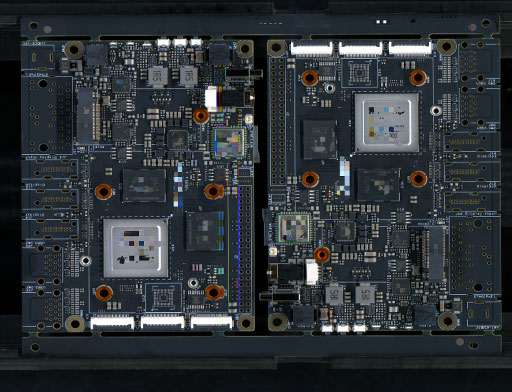
Operating in such extreme environments, the hardware carrier for AI processors—the printed circuit board (PCB) and its surface-mount assembly (PCBA) process—has evolved beyond traditional electronic assembly. It has transformed into a cutting-edge systems engineering discipline that integrates materials science, microelectronics, thermodynamics, electromagnetic field theory, and precision mechanical manufacturing.
Even minor manufacturing defects or process deviations can lead to degraded signal integrity (SI), a collapse in power integrity (PI), thermal stress failures, or even catastrophic chip burnout. Therefore, a deep analysis of the core elements of AI processor PCB assembly—ranging from base materials and high-density interconnect (HDI) design to precision SMT placement and thermal management integration—is crucial for ensuring the high reliability and long-term stability of computing hardware.
I. Key Technologies for AI Processor PCB Design and Substrate Manufacturing
The high-speed and high-current nature of AI hardware places extreme demands on the physical and electrical performance of PCB substrates. As the foundational step preceding assembly, the quality of PCB manufacturing directly determines the success or failure of the subsequent surface-mount process.
High-Density Interconnect (HDI) and Any-Layer HDI Technology
Due to the extremely high pin density of AI processor packages—where Ball Grid Array (BGA) pitches are shrinking to the 0.65mm or even 0.4mm level—traditional through-hole PCBs can no longer meet the requirements for dense routing.
- Buried and Blind Via Technology: AI processor motherboards commonly utilize advanced HDI structures, such as Any-Layer HDI or high-order build-up structures (e.g., 3+N+3, 4+N+4, or higher). Laser Direct Imaging (LDI) is employed to create microvias for layer-to-layer interconnection, with via diameters typically controlled to within 75 microns or even 50 microns.
- Stacked Via Process: To achieve the shortest signal transmission paths and minimize parasitic inductance, multi-layer blind vias must utilize a stacked via design. This necessitates a copper filling process that achieves a high degree of fill integrity—avoiding dimples or voids within the vias—as such defects could easily lead to micro-cracks under the thermal shock of subsequent multiple reflow soldering cycles.
Ultra-High-Speed Material Selection: Low Dielectric Constant (Low Dk) and Low Dissipation Factor (Low Df) Resin Systems
In high-frequency signal transmission operating in the tens of gigahertz (GHz) range, the dielectric properties of the substrate directly determine signal transmission speed and the extent of signal attenuation.
- Resin and Glass Fiber Cloth Matching: Traditional FR-4 materials suffer from high signal loss and severe phase distortion when handling the high-speed SerDes channels found in AI processors.
- Consequently, high-frequency, high-speed copper-clad laminates (CCL) featuring ultra-low dielectric constants (Dk < 3.4 or lower) and ultra-low dissipation factors (Df < 0.003) must be selected—such as those based on specially modified epoxy resins, polyphenylene oxide (PPO), or polytetrafluoroethylene (PTFE) composites.
- Low-Roughness Copper Foil (Low Profile Copper Foil): Conductor loss becomes the dominant factor at high frequencies. Ultra-low profile (VLP) or hyper-low profile (HVLP) electrolytic copper foils must be used to minimize the additional resistance caused by surface roughness—which exacerbates the “skin effect” in high-frequency currents—thereby ensuring the data throughput capabilities of the AI processor’s high-speed buses.
Control of Extreme Layer Counts and Aspect Ratios
- AI processor motherboards often require the integration of complex power distribution networks (PDNs) and numerous signal routing layers, causing the total PCB layer count to soar to 24, 32, or even over 40 layers.
- Aspect Ratio Challenges: In ultra-thick backplanes or high-layer-count motherboards, the board thickness-to-hole diameter ratio for mechanical drilling often exceeds 15:1 or even 20:1. This places immense demands on the optimization of drilling parameters (spindle speed and feed rate), the effectiveness of hole-wall desmearing, and the deep-plating capabilities of both electroless and electrolytic copper processes.
- Micro-crack Prevention: Uneven copper thickness or residual processing chemicals within the via can lead to thermal stress concentration, causing the copper plating inside the via to fracture during the high-temperature stages of assembly reflow soldering. Real-time current density monitoring and additive optimization are essential to ensure uniform copper thickness on the via walls (with an average thickness of no less than 20–25 microns).
II. Co-design of Packaging Substrates and PCBs, and Fine-Pitch Interconnects
The core of an AI processor is often mounted directly onto a substrate or motherboard using Flip Chip technology; this ultra-high-density interconnect method is a critical priority during the assembly phase.
Flip Chip BGA and 2.5D/3D Heterogeneous Integration Substrate Technology
Modern high-performance AI accelerator cards widely adopt Chiplet architectures, integrating compute chiplets, HBM (High Bandwidth Memory), and I/O chiplets via an interposer (such as a silicon interposer or RDL bridge).
- Micro-bump Technology: Interconnects between chiplets and substrates utilize micron-scale copper pillar bumps combined with lead-free solder (e.g., SAC305 or SnAg), with pitches reduced to the 40–55 micron range. Such ultra-fine pitches impose sub-micron alignment accuracy requirements on placement equipment.
- Coordinated Warpage Control: Significant differences in the Coefficient of Thermal Expansion (CTE) exist between silicon, organic substrates, and PCBs (silicon’s CTE is approximately 2.6 × 10⁻⁶/K, whereas organic PCBs can exceed 14 × 10⁻⁶/K in the X/Y directions), generating immense shear stress during thermal cycling. Consequently, PCB stack-up designs must employ symmetrical routing and core materials with balanced CTEs to suppress overall warpage.
Fine-Pitch Pad Design and Surface Finish Processes
For the BGA area on the motherboard that hosts the AI processor package, pad design directly impacts solder joint reliability.
- Solder Mask Pattern Design: An optimized combination of Solder Mask Defined (SMD) and Non-Solder Mask Defined (NSMD) patterns is commonly used. For ultra-fine-pitch BGAs, NSMD pads are generally preferred to provide better mechanical stress relief and prevent stress concentration at the base of the solder joint.
- Surface Finish Selection: Traditional Hot Air Solder Leveling (HASL) has been completely phased out due to poor surface flatness. While Electroless Nickel/Immersion Gold (ENIG) offers good flatness, it carries a risk of “Black Pad” defects; high-end AI motherboards now favor Electroless Nickel/Electroless Palladium/Immersion Gold (ENEPIG) or Organic Solderability Preservative (OSP) to ensure excellent solder wettability and prevent embrittlement caused by excessively thick intermetallic compounds (IMC).
Underfill and Capillary Flow Process Control
Underfill is an essential assembly step to mitigate solder joint fatigue caused by the CTE mismatch between large AI chips and the PCB.
- Capillary Underfill (CUF): Following reflow soldering, a low-viscosity, high-flowability epoxy resin composite is dispensed along the chip’s edge, utilizing capillary action to fill all micro-gaps beneath the chip.
- Curing Parameter Control: The curing temperature profile and viscosity specifications of the underfill must be strictly matched with the particle size distribution of the filler (silica microspheres). Excessively rapid curing can induce internal stress; meanwhile, uneven filling or residual air bubbles can lead to moisture absorption and swelling in high-temperature, high-humidity environments, resulting in chip delamination or solder joint fracture during service.
III. Key Challenges and Process Control in AI Processor SMT Assembly
AI processor motherboards (such as server motherboards and accelerator cards) are typically large in size and thickness, feature extremely high component density, and incorporate numerous components with very high thermal mass. These characteristics pose significant challenges for Surface Mount Technology (SMT) processes.
Reflow Profile Optimization for Extra-Large, High-Thermal-Mass PCBs
AI server motherboards often exceed 400 mm × 500 mm in size and weigh several kilograms; they also feature thick copper foil, including multiple power layers of 2 oz or even 3 oz copper.
- Temperature differentials caused by uneven thermal mass: Chip areas concentrate high-density pin arrays and massive copper structures, whereas edge areas have lower thermal mass. In the reflow oven, excessive heating rates or improper zone settings can cause localized thermal lag, leading to defects such as “cold joints” or “false joints” (poor wetting), or causing PCB delamination and warping due to excessive thermal stress.
- Optimization for multi-zone forced-convection reflow ovens: A nitrogen-purged (O₂ < 50 ppm) reflow oven with at least 10 heating zones is required. By precisely extending the duration in the soaking zone, the surface temperature of the entire large PCB achieves thermal equilibrium (keeping the temperature differential within ±3°C). The assembly then transitions to the peak zone with a gradual ramp rate; the peak temperature is precisely controlled to 20–25°C above the liquidus temperature (typically between 235°C and 245°C), with the dwell time strictly limited to 60–90 seconds to prevent excessive growth of intermetallic compounds (IMCs).
Ultra-Fine Pitch Components and High-Density Stencil Design
In addition to the core AI processor, the motherboard hosts a vast number of passive components (such as micro-decoupling capacitors in 01005 or 0201 packages) and high-density connectors. Step Stencils and Nano-coatings: Large BGA areas require substantial solder paste volume to ensure mechanical strength, whereas surrounding miniature decoupling capacitors require minimal paste to prevent bridging. Consequently, step stencils—manufactured using laser cutting combined with electropolishing and nano-coating—must be employed.
Aperture Ratio Optimization: For components with 0.3mm or 0.4mm pitch, the Area Ratio and Aspect Ratio must exceed 0.66 and 1.5, respectively. When paired with high-thixotropy, low-voiding, no-clean lead-free solder paste (such as SAC305 Type 4 or Type 5 powder), this ensures clean stencil release, eliminating issues like insufficient solder, solder peaking, or slump.
Warpage Control and Dynamic Stress Relief for Complex Components
AI processors and their associated Power Management ICs (PMICs) and high-speed Retimer chips often feature package sizes exceeding 45mm × 45mm. During thermal cycling in the soldering process, they are highly susceptible to “bimetallic strip effect” warpage.
- Precision Pressure Control during Placement: When pick-and-place machines handle large BGAs, the Z-axis downward travel and placement pressure must utilize closed-loop feedback control to prevent excessive mechanical force from crushing the miniature solder balls underneath.
- Support Fixture (Carrier) Design: For extra-large PCBs undergoing reflow, custom high-precision, heat-resistant synthetic stone (Durostone) or titanium alloy support bases are required. Adjustable support pins must be positioned at critical stress points on the underside of the board to prevent sagging due to the PCB’s own weight when it softens at high reflow temperatures, thereby completely eliminating the risk of solder joint separation or displacement caused by gravity.
IV. Power Integrity (PI) and Thermal Management Assembly for High-Power AI Chips
AI processors exhibit immense power consumption and extremely rapid dynamic fluctuations (intense dI/dt), making the assembly of the Power Distribution Network (PDN) and the integration of thermal management systems critical factors in the overall success of the hardware.
High-Current, Low-Voltage (VRM/DrMOS) Layout and Busbar Assembly
To minimize voltage drop (IR drop) and parasitic inductance, the voltage regulator module (VRM)—comprising the multi-phase PWM controller, DrMOS, and high-power inductors—supplying power to the AI processor core must be placed in close proximity to the processor.
- High-Power Inductor and MOSFET Soldering: These power components are bulky, feature thick leads, and possess large bottom thermal pads. During assembly, voiding frequently occurs at these thermal pads. Voids cause a sharp increase in local thermal resistance, leading to hotspots and potential component burnout.
- Voiding Control Standards: The voiding rate beneath power components must be strictly controlled to below 10% (or even under 5%) by optimizing stencil aperture designs (using a grid-like pattern with an aperture ratio of 50%–75%) and employing vacuum-assisted reflow soldering technology.
- Busbar and Copper Pillar Assembly: For AI server motherboards handling input currents of several hundred amperes, standard PCB copper foil thickness is insufficient. Consequently, thick copper busbars must be attached directly to the PCB’s power distribution terminals during assembly using bolting or laser welding processes.
Implementation of Embedded Capacitors and Decoupling Networks
To suppress high-frequency noise and ensure robust transient response, hundreds or even thousands of high-capacitance Multi-Layer Ceramic Capacitors (MLCCs) must be deployed on the motherboard surface and within the AI processor package.
- High-Density Placement of Miniature Capacitors: Hundreds of 0201 or 01005-sized capacitors are often densely packed within cavities on the back of the package. Given the extremely tight spacing, pick-and-place machines require high-speed visual alignment and micron-level correction capabilities.
- Prevention of Micro-cracking: MLCCs are made of brittle ceramic material. If the PCB is subjected to mechanical stress after assembly—such as during depaneling, screw tightening, or heatsink press-fitting—invisible micro-cracks can easily form in the capacitor body, potentially leading to power supply short circuits. Therefore, stress-free methods such as laser depaneling or router-based milling must be used; traditional punching or snap-off depaneling machines are strictly prohibited.
Precision Press-fitting of Vapor Chambers, Liquid Cooling Plates, and High-Thermal-Conductivity TIMs
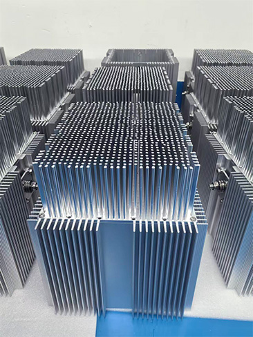
The heat flux of AI processors can reach hundreds of watts per square centimeter, making air cooling alone insufficient; liquid cooling and high-efficiency vapor chambers have become standard features.
- Application and Dispensing of Thermal Interface Materials (TIM): High-performance TIMs—such as phase-change materials (PCM), liquid metal, or high-thermal-conductivity thermal grease—must be evenly applied between the AI chip surface and the heatsink. While liquid metal offers extremely high thermal conductivity, it is electrically conductive and corrosive; consequently, the dispensing process and the assembly of anti-overflow dams require aerospace-grade precision.
- Design of Uniform Clamping Structures: Fastening the heatsink retention mechanism must strictly adhere to specified torque requirements and diagonal tightening sequences. Excessive pressure can crush the silicon chip, while insufficient pressure increases contact thermal resistance. High-precision torque wrenches or automated pneumatic press-fit machines are used to ensure that the pressure applied to the AI chip’s Integrated Heat Spreader (IHS) is evenly distributed, with tolerances controlled within ±5%.
V. Quality Control, Non-Destructive Testing (AOI/X-Ray/3D CT), and Reliability Verification
Given the extremely high value of AI processor motherboards and their complex assembly structures, traditional visual inspection and electrical testing (ICT/FCT) are inadequate for examining internal BGA solder joints and the internal architecture of multilayer boards. A multi-dimensional, end-to-end non-destructive testing system must be established.
Early-Stage Detection via 3D AOI and 3D SPI
- 3D Solder Paste Inspection (SPI): Real-time scanning of solder paste height, volume, and area during the printing process to intercept defects such as insufficient paste, excessive paste, or misalignment.
- 3D Automated Optical Inspection (AOI): Comprehensive inspection of all surface-mount components—checking for missing parts, misalignment, polarity reversal, tombstoning, and solder joint surface defects—using multi-angle structured light and AI-based image recognition algorithms before and after reflow soldering.
High-Resolution 3D X-ray Inspection (AXI) and Industrial CT Technology
- 3D Internal Solder Joint Visualization: High-resolution 3D AXI (micro-focus X-ray inspection) is employed for non-destructive penetration analysis of complex structures, such as AI processor BGAs, flip-chip bumps, and bottom thermal pads on power devices.
- Quantitative Analysis of Voiding and Bridging: Computed Tomography (3D CT) reconstruction technology enables precise, cross-sectional calculation of void percentages, shapes, and the presence of cracks or cold joints within individual solder balls, ensuring 100% quality compliance for hidden solder joints.
Environmental Stress Screening (ESS) and Reliability Verification
AI hardware must undergo rigorous Environmental Stress Screening (ESS) prior to shipment to expose potential early-life failures (infant mortality).
- Highly Accelerated Stress Screening (HASS) and Highly Accelerated Life Testing (HALT): Assembled AI accelerator cards are subjected to combined environments featuring extreme temperature change rates (>60°C/min) and multi-axis random vibration to simulate product limits under extreme transport conditions and high-load server room operations.
- Combined Thermal-Electrical Burn-in Testing: Dynamic burn-in tests lasting hundreds of hours are conducted under high-temperature, full-load power conditions. Parameters such as core voltage droop, temperature drift, and Soft Error Rate (SER) are monitored to ensure the product meets zero-defect, industrial-grade reliability standards before delivery to end-users.
VI. Future Trends: Technological Evolution and Development Directions in AI Processor Hardware Manufacturing
As the pace of Moore’s Law slows, the scaling of AI computing power increasingly relies on breakthroughs in advanced packaging and System-in-Package (SiP) technologies; this, in turn, compels PCB and assembly processes to evolve toward higher levels of integration.
Introduction of Glass Substrates and Assembly Transformation
When dealing with ultra-large, ultra-high-density AI chips, traditional organic resin substrates are approaching their physical limits regarding flatness and the coefficient of thermal expansion (CTE). Glass substrates offer ultra-flat surfaces, excellent dimensional stability, and tunable CTE, enabling the support of higher-density Through-Glass Vias (TGV). In the future, precision micro-soldering, laser cutting, and micro-via metallization associated with glass substrates will become key battlegrounds in the assembly sector.
Adoption of Hybrid Bonding Technology
The transition from traditional micro-bumps to direct copper-to-copper (Cu-Cu) hybrid bonding will shrink interconnect pitches from the micrometer scale to the sub-micrometer scale (<1 μm). This drastically reduces electrical connection impedance between the chip and the substrate while exponentially increasing signal transmission bandwidth. Consequently, assembly equipment must possess nanometer-level visual alignment capabilities and ultra-clean environmental control (Class 1 cleanroom standards).
Intelligent Digital Twins and AI-Driven Assembly Optimization
On the manufacturing front, the integration of edge computing, machine vision, and AI algorithms enables the creation of a comprehensive digital twin model covering the entire process—from solder paste printing and thermal zone adjustment to dispensing and curing.
The system can automatically fine-tune reflow profiles, placement pressure, and dispensing trajectories based on real-time environmental parameters. This achieves true adaptive intelligent manufacturing, pushing the yield and reliability of AI processor hardware to unprecedented levels.
In summary, AI processor PCB assembly is a highly complex, multidisciplinary system engineering endeavor. Every step is inextricably linked—from the selection of advanced, high-performance materials and the manufacturing of high-order HDI boards to the precision placement of fine-pitch flip-chips, the integrated management of high-power signal integrity and thermal performance, and finally, rigorous non-destructive testing and reliability validation.
Only through meticulous process control and technological innovation across the entire workflow can we establish a rock-solid hardware foundation for the explosive global demand for AI computing power.