
High-Speed, High-Frequency PCB Assembly Factory: Precision Manufacturing and PCBA Solutions for High-Speed Signal Transmission.
The challenges in manufacturing high-speed, high-frequency PCBs extend beyond simply increasing circuit density or shortening signal paths; the core difficulty lies in establishing stable engineering synergy across PCB design, material selection, impedance control, precision assembly, and product testing.
With the advancement of high-speed communications, AI servers, network switching equipment, radar systems, and high-performance computing devices, the PCB has evolved from a traditional carrier for electrical connections into a critical component that directly influences overall system performance.
For high-speed, high-frequency electronic products, the precision of PCB fabrication and the quality of PCB assembly are often the deciding factors in whether signals can maintain their integrity and stability within complex circuit environments.
High-Speed, High-Frequency PCB Assembly: The Real Challenge Lies in Signal Integrity
High-speed digital signals and high-frequency analog signals impose more rigorous requirements on PCB architecture. As signal frequencies and transmission rates continue to rise, even minor manufacturing deviations—which might be negligible in standard PCB assembly processes—can translate into significant electrical performance issues.
Key areas of focus include:
Impedance Continuity
High-speed signal lines typically require precise control of characteristic impedance—for instance, 50Ω for single-ended signals and 100Ω for differential signals. Factors such as trace width, dielectric thickness, copper foil thickness, and the structure of reference planes all influence the final impedance.
Signal Loss and Crosstalk Control
In high-frequency environments, dielectric loss, conductor loss, and electromagnetic coupling between adjacent traces can degrade signal quality. Utilizing low-loss materials, maintaining optimal trace spacing, ensuring continuous reference planes, and implementing proper grounding designs are essential strategies for mitigating these issues.
Connectors and Via Structures
High-speed signals are prone to impedance discontinuities at connectors, vias, and layer-transition points. For high-density interconnect (HDI) designs, techniques such as back-drilling, the use of blind and buried vias, and the optimization of via pads and anti-pads are necessary to minimize unwanted parasitic effects. These issues cannot be resolved solely during the back-end assembly stage; they require comprehensive control across the phases of PCB design, substrate fabrication, and SMT manufacturing.
Key Processes in High-Speed/High-Frequency PCBA Manufacturing
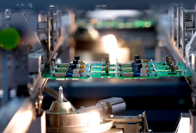
The production requirements for high-speed/high-frequency PCB assemblies differ significantly from those for standard consumer electronics. Components with fine pitches, high pin densities, and high-speed interface chips, in particular, demand greater precision in assembly and higher consistency in soldering.
① Precision SMT Placement
High-speed communication chips, RF components, and BGA-packaged devices typically require high placement accuracy. During production, parameters such as solder paste printing, placement pressure, and reflow temperature profiles must be optimized—taking into account component packaging, pad dimensions, and any potential PCB warpage.
② Reflow Soldering Thermal Management
Multilayer high-speed PCBs may incorporate a combination of different dielectric materials, each with distinct heat capacities and thermal expansion characteristics. Reflow soldering processes must be tailored to the specific board structure and the thermal sensitivity of the components to prevent issues such as solder voids, cold joints, bridging, and thermal damage to the components.
③ Solder Quality and Micro-Defect Inspection
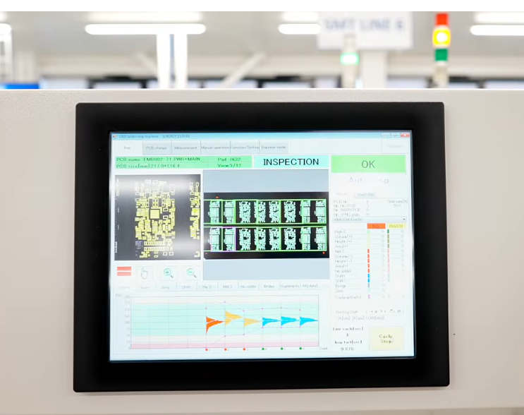
For components like BGAs, QFNs, and those with hidden solder joints, visual inspection alone is insufficient to fully assess solder quality. A combination of 3D AOI (Automated Optical Inspection), X-ray inspection, and electrical testing is typically required to verify solder joint integrity and detect bridging, voids, or other assembly defects.
④ ESD and Cleanliness Control
RF front-end modules, communication chips, and other highly sensitive electronic components are susceptible to damage from electrostatic discharge (ESD) and contamination. The production environment must implement robust ESD protection, strict material storage protocols, and rigorous cleanliness controls to minimize the risk of potential failures.
From Materials to Testing: Systematic Engineering Validation for High-Speed/High-Frequency PCBs
The performance of high-speed/high-frequency PCBs cannot be determined by simple continuity testing alone. A reliable PCBA manufacturing solution must integrate material properties, circuit architecture, and final electrical performance.
| Engineering Process | Key Control Requirements |
| PCB Materials | Low-loss dielectric materials, dielectric constant stability, and material consistency |
| Circuit Structure | Impedance tolerance, differential routing, and reference plane continuity |
| PCB Fabrication | Layer-to-layer alignment, hole wall quality, copper thickness, and trace accuracy |
| SMT Assembly | Solder paste printing, component placement accuracy, and reflow soldering profiles |
| Quality Inspection | AOI, X-Ray, ICT, and functional testing |
| Performance Verification | TDR impedance testing, S-parameter testing, and signal integrity analysis |
It should be emphasized that TDR (Time-Domain Reflectometry) and S-parameter testing cannot simply be replaced by conventional PCBA electrical testing. For high-speed interfaces and RF circuits, appropriate test fixtures, calibration protocols, and verification standards must be configured based on specific product requirements.
KingTop Technology: A Partner for High-Speed/High-Frequency PCB and PCBA Manufacturing
KingTop Technology specializes in PCB manufacturing and PCBA electronic assembly services, providing support for sectors such as industrial control, telecommunications equipment, smart electronics, automotive electronics, and high-performance computing.
When handling high-speed/high-frequency PCB projects, KingTop Technology focuses on product engineering requirements—integrating PCB design data, material properties, manufacturing processes, and assembly quality—rather than treating PCB fabrication and SMT assembly as isolated production stages.
Their services include:
PCB Manufacturing and Customization: Support for multi-layer PCBs, high-density interconnects (HDI), and custom manufacturing using a variety of material systems.
SMT and Precision Assembly: Services for surface-mount technology (SMT), BGA, and the assembly of other precision components.
Engineering and DFM (Design for Manufacturability) Support: Evaluation of Gerber files, BOMs, placement files, and production processes to ensure manufacturability.
Quality Inspection: Implementation of SPI (Solder Paste Inspection), AOI (Automated Optical Inspection), X-ray inspection, and electrical testing tailored to product requirements.
Custom PCBA Solutions: Development of manufacturing strategies based on specific product applications, production volume requirements, and performance metrics.
For high-speed/high-frequency products, KingTop Technology prioritizes pre-manufacturing engineering communication—covering critical component packaging, pad design, board stack-up, assembly processes, and testing requirements—to help clients identify potential manufacturing risks before full-scale mass production begins.
What Should You Look for When Choosing a High-Speed/High-Frequency PCBA Manufacturer?
Evaluating a manufacturer for high-speed/high-frequency PCBs requires looking beyond the number of SMT machines or production speed. The true differentiator is the manufacturer’s ability to understand the electrical requirements of high-speed circuits and translate them into actionable, verifiable manufacturing standards.
It is recommended to focus on three key areas:
Engineering Expertise: Does the manufacturer possess engineering experience in impedance control, material selection, signal integrity, and the assembly of high-speed components?
Process Control Capability: The ability to develop sound assembly, soldering, and inspection processes tailored to various PCB structures.
Quality Verification Capability: The ability to provide verification support—covering impedance, solder joint quality, and electrical performance—in accordance with specific product requirements.
Competition in the manufacturing of high-speed, high-frequency PCBs is no longer limited to circuit precision or assembly efficiency; rather, it hinges on the collaborative capability across the entire electronics manufacturing chain.
KingTop Technology is dedicated to integrating PCB manufacturing, precision PCB assembly, and engineering technical support. We provide our clients with highly reliable manufacturing solutions for high-speed, high-frequency electronics, facilitating the transition from design validation to stable, full-scale production.