The explosive growth of Artificial Intelligence (AI) and High-Performance Computing (HPC) chips is profoundly reshaping the boundaries of modern microelectronic packaging and circuit board manufacturing technologies.
Contemporary flagship AI processors often integrate tens or even hundreds of billions of transistors, forming massive computational cores through the use of High-Bandwidth Memory (HBM) and advanced packaging technologies.
Amidst this architectural evolution, traditional packaging and Surface Mount Technology (SMT) can no longer meet the operational demands associated with power densities ranging from hundreds of watts to the kilowatt level.
Flip-chip packaging—serving as the pivotal hub for chip-level interconnects—is increasingly exhibiting a trend of unprecedented deep coupling and co-design with Printed Circuit Board (PCB) assemblies, which manage system power delivery and high-speed signal distribution.
I. Deep Architecture and Technological Evolution of AI Processor Flip-Chip Packaging
Modern AI processors (such as large-scale GPUs, AI accelerators, and Neural Processing Units) widely employ heterogeneous integration and 2.5D/3D advanced packaging architectures. Flip-chip packaging acts as a critical bridge, establishing efficient electrical connections between active components and the package substrate.
Bump Pitch Scaling and Interconnect Metallurgy
As AI processors evolve toward higher I/O densities, traditional micro-bump pitches have scaled down from the early 40-micron range to 25 microns or less; some cutting-edge experimental structures have even adopted hybrid bonding (direct copper-to-copper bonding), resulting in exponential growth in interconnect density.
- Bump Materials: There has been a comprehensive shift away from traditional tin-lead (SnPb) or high-lead bumps toward lead-free solder pastes (such as SAC305) and copper pillars topped with a small amount of solder (capping). Copper pillars provide excellent mechanical support height, preventing short or open circuits caused by thermo-mechanical stress during thermal cycling.
- Intermetallic Compound (IMC) Control: During the reflow process of flip-chip solder joints, the interdiffusion of copper and tin leads to the formation of Cu₆Sn₅ and Cu₃Sn intermetallic compounds. Excessive thickness or brittleness in the IMC layer creates zones of stress concentration; therefore, precise temperature profile control and barrier layer plating processes (such as Ni/Au or Ni/Pd/Au) are essential to strictly limit the IMC thickness to a stable range.
Technical Challenges of Flip-Chip Substrates
Flip-chip substrates for AI processors typically utilize high-end Ajinomoto Build-up Film (ABF) materials, featuring multi-layer fine circuitry (with line/space dimensions reduced to below 2/2 µm) and dense micro-via structures.
- Coefficient of Thermal Expansion (CTE) Mismatch Challenge: There is a significant disparity in the CTE between the silicon die (CTE ≈ 2.6 × 10⁻⁶/K) and the organic resin substrate (CTE ≈ 15 × 10⁻⁶/K). When the AI chip switches between high-speed computing and low-load states, drastic temperature fluctuations generate intense shear stress on the peripheral solder bumps.
- Synergistic Optimization of Underfill and Molding Compounds: To dissipate thermomechanical stress between the die and the substrate, Capillary Underfill (CUF) or Molded Underfill (MUF) materials must possess a high glass transition temperature (Tg > 175°C), a low CTE, and excellent flowability to completely fill the micron-scale gaps between bumps and eliminate voids.
II. System Integration and Physical Challenges at the PCB Assembly Level
Once the flip-chip packaging is complete, the entire high-power AI processor module must be soldered onto a motherboard or an accelerator card PCB using Ball Grid Array (BGA) or Column Grid Array (CGA) interconnects. In this context, PCB assembly goes beyond mere mechanical fastening and electrical connection; it directly determines the limits of power integrity (PI), signal integrity (SI), and thermal management for AI systems.
High-Layer-Count and High-Density Interconnect (HDI) PCB Design
AI server motherboards and accelerator cards typically require designs with 20 to over 30 layers, extensively utilizing Any-layer HDI and back-drilling technologies.
- Signal Loss Suppression: High-speed interfaces between AI chips (such as PCIe Gen 6/Gen 7 and SerDes links operating at tens or even hundreds of Gbps) are extremely sensitive to dielectric loss (Df). PCB substrates must employ special combinations of epoxy resin and glass fiber cloth with ultra-low or extremely low loss characteristics (e.g., modified PPE or PTFE-based materials) to maintain adequate eye diagram opening for high-frequency signals transmitted over long traces.
- Power Distribution Network (PDN) Optimization: Sudden peak current surges in AI processors (with di/dt rates reaching thousands of amperes per second) can cause severe voltage droop. The PCB’s inner layers must incorporate large-area, ultra-thin power and ground copper planes (e.g., 0.5 oz or 1 oz) and accommodate a vast number of high-frequency ceramic capacitors (MLCCs) around the chip to minimize PDN impedance.
SMT Assembly Process and Solder Joint Reliability Control
Surface-mounting large, heavy AI processor flip-chip modules (including the heatsink retention mechanism) onto the PCB presents a demanding process window for SMT manufacturing:
- Printing Precision and Stencil Design: For fine-pitch BGA pads, stencil aperture thickness and shape must be optimized using nano-coatings and micro-fluid dynamics. This ensures a stable 100% solder paste release rate, preventing defects such as insufficient solder (leading to open circuits) or excessive solder (causing adjacent pin shorts).
- Solder Joint Creep Resistance: AI servers operate in high-temperature, high-load environments for extended periods, making solder joints susceptible to high-temperature creep. The choice of lead-free solder paste alloy composition (such as composite alloys incorporating trace elements like silver, bismuth, or antimony) and the control of crystalline structures via reflow peak temperatures directly determine the field failure rate (FR) of servers over their multi-year lifecycles.
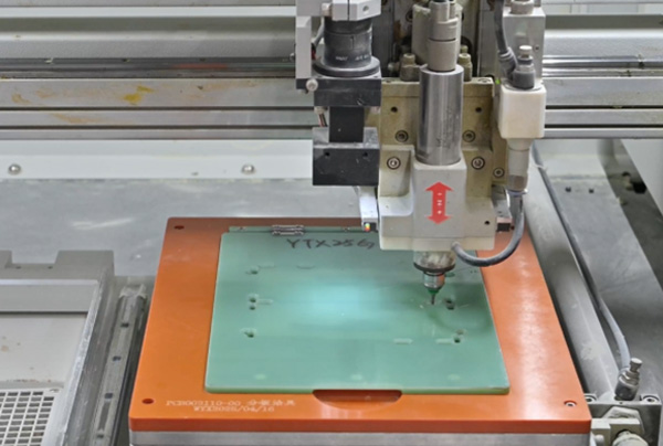
III. Thermo-mechanical Stress, Warpage, and the Cooling Revolution
The power density of AI processors has skyrocketed from the tens of watts per square centimeter seen in early designs to over a kilowatt for a single package today. The coupling of thermal and mechanical stresses represents the most destructive factor across the entire chain, from flip-chip packaging to PCB assembly.
Managing Multi-scale Warpage in Packages and PCBs
Bimetallic effects and residual stress: From upstream wafer-level packaging, reflow cooling, and underfill curing to final board-level SMT reflow, variations in cooling rates during each thermal process leave residual thermal stresses across the differing material layers of the chip, substrate, and PCB.
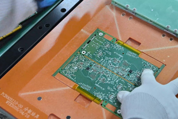
Dynamic warpage compensation: During the board-level SMT heating phase (reflow zone), PCBs and package substrates undergo non-linear warpage driven by differences in the coefficient of thermal expansion (CTE). Excessive warpage can cause peripheral BGA solder balls to lift (lose contact) or fail to fuse properly, resulting in “Head-in-Pillow” (HiP) defects or cold joints. Senior process engineers must mitigate deformation through precise temperature profile optimization—such as extending the soak zone and controlling the ramp-up rate—and by employing appropriate support fixtures on the underside of the PCB.
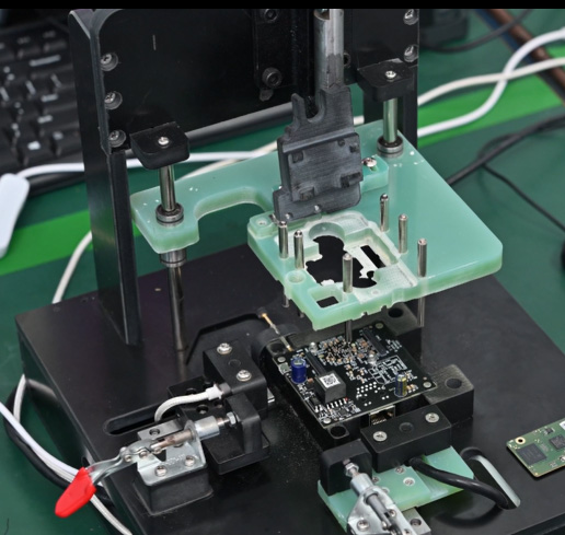
Synergy Between High-End Thermal Architectures and PCB Structures
Vapor chambers (VC) and liquid cooling interfaces: Most high-end AI processors utilize liquid cooling designs featuring either an integrated heat spreader (IHS) or direct die cooling. Thermal retention mechanisms exert mechanical downward pressure of up to several hundred newtons on the package surface; this immense static and dynamic load is transmitted directly to the flip-chip substrate and exerts downward pressure on the PCB.
Localized PCB Rigidity Reinforcement: To prevent permanent downward deformation (bow and twist) of the PCB under the immense pressure of mounting hardware, metal stiffeners are often embedded within the PCB, or high-strength backplanes are designed for the rear side. This ensures that the micro-solder joints between the substrate and the PCB do not fracture due to prolonged exposure to excessive shear stress.
IV. Advanced Manufacturing Inspection and Quality Assurance Systems
Given the high value and structural complexity of AI chip modules, traditional visual inspection or conventional electrical testing is no longer sufficient to guarantee yield rates. Comprehensive non-destructive testing and closed-loop quality control systems must be implemented.
High-Resolution 3D X-ray Inspection (3D X-ray / CT)
Micro-bumps within the flip-chip assembly and blind vias in the substrate cannot be directly observed from the outside. Nanoscale 3D X-ray computed tomography (CT) is required to perform non-destructive cross-sectional reconstruction of the package interior, enabling precise detection of defects such as bridging, voids, cracks, or micro-fractures caused by thermal stress.
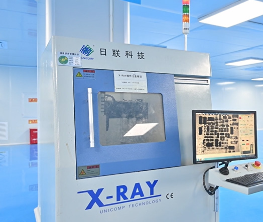
For the solder joints beneath large BGA arrays on assembled PCBs, 3D AOI (Automated Optical Inspection) and 3D AXI (Automated X-ray Inspection) are used for full-scale inspection, automatically identifying defects related to the volume, height, and coverage of hidden solder joints.
Digital Twin and Process Simulation
Prior to physical pilot production, the development of modern, high-end AI hardware relies heavily on multi-physics co-simulation:
Using Finite Element Analysis (FEA) to simulate transient thermal distribution during chip operation.
Inputting thermal distribution data into mechanical stress models to predict the fatigue life (accumulated plastic strain) of flip-chip bumps and PCB solder joints under extreme operating cycles.
Utilizing digital twin technology to adjust trace density, copper distribution, and stiffener placement during the early design phase, thereby avoiding manufacturing pitfalls at the source.
V. Conclusion
The flip-chip packaging and PCB assembly of AI processors have long since transcended the scope of traditional electronics manufacturing, evolving into a highly interdisciplinary field of system-level microelectronics engineering. Every stage—from nanoscale chip-bump metallurgy and micron-scale ABF substrate routing to millimeter-scale high-frequency multilayer PCB design and macro-level thermal management—is inextricably linked.
Only by co-optimizing the chip, package, substrate, PCB, and thermal systems as an indivisible, integrated whole during the initial design phase, while strictly controlling material interface reactions and thermomechanical stresses during manufacturing, can the long-term stability and reliability of next-generation AI hardware be ensured amidst the race for extreme computing power.
FAQs
Why do AI processor flip-chip packages replace traditional solder bumps with copper pillars?
A: As the I/O density of AI chips skyrockets, traditional micro-bumps are prone to bridging shorts during reflow due to insufficient height or small volume. Copper pillars provide superior mechanical support height, along with better current-carrying capacity and electromigration resistance, effectively supporting stable electrical interconnections under high power density conditions.
How is the Coefficient of Thermal Expansion (CTE) mismatch between the flip-chip substrate and the silicon die addressed?
A: There is a significant difference in CTE between the silicon die and the organic resin substrate, which generates strong shear stress during drastic temperature fluctuations. The industry primarily addresses this by introducing Capillary Underfill (CUF) or Molded Underfill (MUF) technologies—featuring high glass transition temperatures (Tg) and low CTE—to completely fill the gap between the die and the bumps, thereby distributing and absorbing thermo-mechanical stress.
Why must high-end AI server PCBs utilize ultra-low-loss materials?
A: High-speed interfaces between AI processors (such as PCIe Gen 6/Gen 7 and SerDes channels operating at tens of Gbps) are extremely sensitive to signal attenuation. Using combinations of specialized epoxy resins and glass fiber fabrics with ultra-low-loss properties—such as modified PPE or PTFE—significantly reduces dielectric loss during high-frequency signal transmission across long traces and multilayer boards, ensuring eye diagram openness and data integrity.
How can “head-in-pillow” (HIP) defects be prevented in large flip-chip modules during the SMT process?
A: During SMT reflow, large AI processor modules often suffer from poor solder joint contact (such as the “head-in-pillow” effect) due to uneven substrate heating or localized warpage. Prevention requires optimizing solder paste release rates using nano-coated stencils, precisely tuning the reflow oven’s temperature profile (including extending the soak zone), and employing support fixtures on the PCB backside to suppress deformation.
What impact does the downward force of up to several hundred Newtons—applied by AI chip retention mechanisms—have on the PCB?
A: Significant static and dynamic downward forces are transmitted directly to the flip-chip substrate and PCB, easily causing permanent PCB deformation (bow and twist) and subsequent micro-solder joint fractures. Therefore, metal stiffeners must be embedded within the PCB, or a high-strength backplate must be designed for the rear side, to distribute mechanical loads.
Why are traditional visual inspections or conventional electrical tests insufficient to ensure the yield of AI chip modules?
A: Modern AI chip architectures are highly complex; the micro-bumps inside the flip-chip package and the blind vias within the multi-layer substrate cannot be directly observed from the outside. Manufacturers must employ nanoscale 3D X-ray computed tomography (3D CT) and 3D automated X-ray inspection (3D AXI) for non-destructive testing to accurately detect internal voids, micro-cracks, and bridging defects in hidden solder joints.
What role does multi-physics co-simulation play in AI hardware R&D?
A: Multi-physics co-simulation enables the use of finite element analysis (FEA) to simulate transient thermal distribution during chip operation prior to physical pilot production. It also predicts the fatigue life and accumulated plastic strain of flip-chip bumps and PCB solder joints under extreme operating cycles, thereby mitigating manufacturing risks at the design stage.