An in-depth analysis of the end-to-end manufacturing process for CM4 carrier board PCBA—a comprehensive technical guide covering everything from design adaptation to mass production delivery.
In the development ecosystem for edge computing, the Industrial IoT (IIoT), smart gateways, and embedded terminal products, the Raspberry Pi CM4 Compute Module has become a mainstream choice for hardware teams looking to bring products to market quickly.
Unlike general-purpose Raspberry Pi development boards, the CM4 integrates the processor, memory, storage, and wireless modules onto a single high-density core module, with all peripheral signals routed through onboard connectors. Developers need only focus on interface definitions, structural integration, and peripheral circuitry for the carrier board to rapidly build fully customized terminal products.
However, after completing schematic and PCB designs, many teams encounter a host of unexpected issues during the PCBA manufacturing stage—ranging from cold solder joints on high-density connectors and excessive power supply ripple to sensor signal drift, low yields in small-batch pilot runs, and widespread rework during mass production.
While these issues may appear to be soldering defects on the surface, they fundamentally stem from a lack of alignment between the design phase and the subsequent manufacturing process. This often leads to the frustrating scenario where a design works perfectly on paper but fails to translate into a high-quality physical product.
For products like CM4 carrier boards—characterized by high component density and complex interfaces—PCBA manufacturing is far more than simply “placing components on a board.” It is a systematic engineering process encompassing DFM (Design for Manufacturability) optimization, NPI (New Product Introduction), end-to-end material management, precision SMT assembly, reliability testing, and mass production iteration.
Especially in an industrial hub like Shenzhen—where hardware manufacturing resources are highly concentrated—selecting the right manufacturing partner and mastering the specific manufacturing challenges of CM4 carrier boards are decisive factors in whether an edge AI product can successfully transition from prototype to stable mass production.
As a benchmark enterprise among China’s top ten turnkey PCB assembly service providers, Shenzhen KingTop Technology Co., Ltd. is deeply rooted in the local electronics manufacturing industry. We are a professional manufacturer specializing in one-stop PCBA services for highly complex single-board designs. The company’s core strengths lie in the successful manufacturing of high-density, high-reliability PCBs, with extensive engineering expertise accumulated in the contract manufacturing of complex mixed-signal boards—such as CM4 expansion boards. We possess a dedicated DFM (Design for Manufacturability) optimization team, high-precision SMT production lines, and comprehensive 3D SPI and X-Ray inspection equipment. We implement customized processes specifically for the 0.5mm-pitch pins of CM4 board-to-board connectors, exercising targeted control over the entire workflow—from stencil aperture design and placement alignment to reflow profiles—to fundamentally minimize common industry defects like cold solder joints and solder bridging.
Leveraging Shenzhen’s mature local electronics supply chain, we rapidly conduct risk assessments and material kitting for the full range of BOM components required for CM4 expansion boards. We provide end-to-end services covering everything from rapid prototyping and small-batch pilot runs to stable mass production, offering hardware clients in the Industrial IoT, smart gateway, and edge computing sectors a turnkey PCBA solution that encompasses collaborative design, precision assembly, and full-function testing.
This article begins with the product positioning of CM4 expansion boards and provides a comprehensive breakdown of the entire PCBA contract manufacturing process. It covers every critical stage—from upfront design optimization, engineering assessment, and material management to precision assembly, testing/verification, and mass production delivery—offering hardware teams a practical, actionable manufacturing guide.
I. Product Characteristics of CM4 Expansion Boards and Core PCBA Manufacturing Challenges
The primary distinction between CM4 expansion boards and standard PCBs is the need for deep synergy between the board’s electrical performance and the CM4 core module. Even minor deviations during any manufacturing step can directly impact the core module’s operation, potentially resulting in functional anomalies in the final device. Consequently, the PCBA manufacturing complexity far exceeds that of standard microcontroller baseboards or general-purpose interface boards; the conventional process systems used by many traditional contract manufacturers are often entirely unsuited to these specific manufacturing requirements.
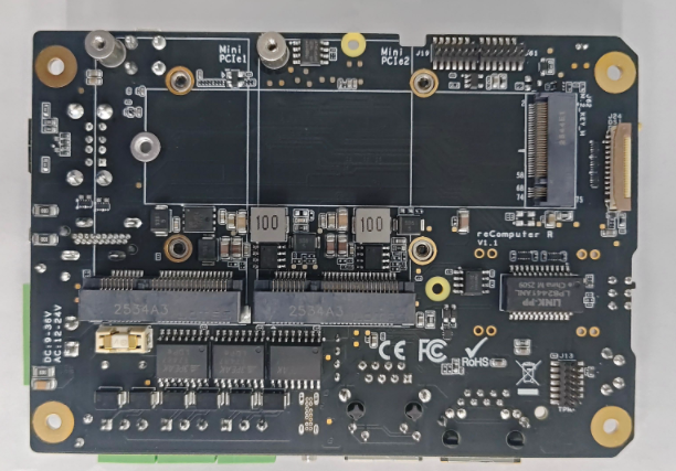
1.1 Assembly Precision Challenges Posed by High-Density Connectors
The CM4 core module connects to the expansion board via two high-density, 2×100-pin board-to-board connectors. These feature a pin pitch of just 0.5mm, with each connector housing 200 pins—totaling 400 pins across the pair. Such high pin density imposes extremely stringent requirements on PCB pad aperture precision, solder paste deposition volume, and component placement accuracy. Even a 0.1mm deviation in pad design or improper control of solder paste volume can easily lead to issues such as solder bridging, cold solder joints, and pin misalignment.
During the manual prototyping phase, many hardware teams manage to solder the connectors using only hot-air guns and microscopes; because the prototype boots up successfully, they often assume the design is sound. However, upon entering small-batch trial production, they frequently discover that over 30% of the boards exhibit issues—such as the CM4 module failing to be recognized, intermittent power loss after startup, or unstable USB signals. Exhaustive troubleshooting eventually reveals that these problems stem from cold solder joints on specific connector pins.
Such defects are notoriously difficult to detect during manual soldering because the manual pressure applied to the connector pins can temporarily mask the cold solder joints; the defects only manifest en masse after the boards undergo shipping or thermal cycling tests.
Even more critically, the CM4 connector array carries a mix of high-speed signals, high-current power pins, and low-voltage differential signals. A cold solder joint on just a single power pin can starve the core module of power, causing random system crashes, reduced computing performance, or abnormal temperature spikes. These faults lack consistent reproduction conditions, making them extremely costly and difficult to diagnose. This is precisely why the PCBA manufacturing process for CM4 expansion boards cannot rely on standard SMT protocols; instead, a specialized process control system must be established specifically to handle these high-density connectors.
1.2 Challenges in Managing Signal and Power Integrity for Mixed-Complexity Circuits
A typical CM4 expansion board is a prime example of a mixed-complexity circuit, integrating three distinct types of signal paths:
- High-speed signals routed from the CM4 module, including PCIe Gen2, USB 2.0/3.0, Gigabit Ethernet RGMII, and MIPI CSI/DSI video signals. These signals typically operate at speeds ranging from hundreds of megabits to several gigabits per second, imposing stringent requirements on trace length matching, impedance control, and reference plane integrity.
- High-power supply rails: The CM4 core module has a peak power consumption of 7.5W; combined with peripheral circuitry on the expansion board, the total peak current exceeds 3A. Even minor impedance deviations along the power path can cause a voltage drop in the core supply, compromising system stability.
- Low-speed analog signals, such as ADC sampling circuits, various sensor inputs, and audio signals. These signals are highly sensitive to power supply noise and spatial electromagnetic interference.
The coexistence of these three signal types—each with vastly different characteristics—on a single expansion board means that any manufacturing process deviation can disrupt the signal integrity balance established during the design phase.
For instance, a “cold solder joint” (poor connection) on a high-current power pad significantly increases equivalent impedance, causing power ripple to exceed the limits validated during simulation. Similarly, if the plating thickness of vias near high-speed signal traces falls short of specifications, trace impedance will deviate from the design value, ultimately leading to an increased bit error rate (BER) for high-speed signals.
Many teams observe normal operation during the prototyping stage but encounter persistently high packet loss rates in Gigabit Ethernet after mass production; fundamentally, this occurs because manufacturing process deviations compromise the original signal integrity design.
1.3 Supply Chain and Process Control Challenges Arising from Diverse Material Types
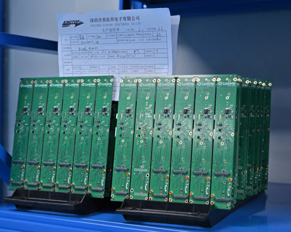
A fully functional CM4 expansion board often features a Bill of Materials (BOM) containing over 200 items with a vast range of package sizes. These include everything from miniature 0201 or even 01005-sized resistors and capacitors to large, irregularly shaped through-hole components like screw terminals, DC jacks, and USB ports, as well as specialized parts such as relays, high-power MOSFETs, and shielding cans.
Materials with different packages impose vastly different requirements regarding SMT placement pressure and reflow soldering temperature profiles; miniature components are prone to “tombstoning” and misalignment, while large components are susceptible to cold solder joints and solder joint cracking.
Even more challenging is the fact that many specialized interface chips and industrial-grade components used in CM4 expansion boards are “long-lead-time” items subject to significant market supply volatility. If the original manufacturer runs out of stock, suitable alternatives must be identified.
If the contract manufacturer’s engineering team lacks sufficient hardware expertise, substituting a component with the same package but different electrical parameters could cause the entire board to fail. For instance, replacing a low-ESR ceramic capacitor intended for a power circuit with a standard general-purpose capacitor could cause power supply ripple to exceed the CM4 module’s tolerance threshold, leading to systemic instability.
1.4 Custom Manufacturing Requirements Driven by Product Diversity
CM4 expansion boards serve a wide array of applications—ranging from industrial I/O control boards and outdoor 5G gateways to interactive baseboards for smart terminals and on-board controllers for rail transit—each with vastly different PCBA reliability requirements.
Consumer-grade applications require only standard room-temperature operation; industrial-grade applications demand reliable performance across a wide temperature range (-40°C to 85°C); and automotive-grade applications must adhere to comprehensive functional safety standards. Consequently, the PCBA manufacturing system cannot apply a “one-size-fits-all” standard to every order; instead, it must flexibly adjust process standards, inspection criteria, and reliability validation protocols based on the product’s specific application scenario.
Many hardware teams manage products characterized by a “long-tail” model involving multiple SKUs: a single base design for a CM4 expansion board might spawn over a dozen variants tailored to different customers through the addition or removal of interfaces and adjustments to component configurations. While this model can significantly reduce R&D and tooling costs, it places extremely high demands on the PCBA contract manufacturer regarding BOM management, production line changeover control, and error-proofing systems; the accidental mixing of different material versions can result in the scrapping of entire batches of products.
II. Pre-production Stages for CM4 Expansion Board PCBA Contract Manufacturing: Aligning Manufacturing Feasibility with Design
Many manufacturing issues associated with CM4 expansion boards actually originate during the design phase. Hardware engineers often export files and send them directly to contract manufacturers after completing schematic and PCB designs, without considering the process constraints of subsequent manufacturing stages. This often forces manufacturers to use standard processes—resulting in extremely low yields—or necessitates repeated design revisions, thereby extending the trial production cycle. Professional CM4 expansion board PCBA services do not begin only upon receipt of Gerber files; instead, they intervene early during the design phase, utilizing Design for Manufacturability (DFM) reviews to eliminate the vast majority of manufacturing risks upfront.
2.1 Key DFM Optimization Points Specific to CM4 Expansion Boards
Given the core characteristics of CM4 expansion boards, DFM reviews must go beyond standard PCB rule checks and focus on targeted optimization across three key dimensions: high-density connectors, power paths, and high-speed signals. First, optimization of pads and stencil apertures for high-density connectors.
The board-to-board connectors used with the CM4 feature extremely fine pin pitches; standard proportional pad designs often lead to solder bridging between adjacent pins. Professional DFM optimization involves slightly shortening the connector pin pads (by 0.1mm) toward the board interior and employing an inset design for stencil apertures. This increases the solder mask clearance between adjacent pads while maintaining sufficient effective soldering area, thereby fundamentally reducing the probability of bridging.
Additionally, precision checks are implemented for connector alignment pins to ensure that alignment errors during SMT placement remain within ±0.05mm, completely preventing misalignment issues. Second, design for manufacturing redundancy in high-current power paths.
During the DFM review stage, every pad, trace width, and via count within the CM4’s core power supply circuit is inspected. This ensures that the current-carrying capacity of each high-current path includes a redundancy margin of over 30%, while also avoiding common manufacturing defects such as incomplete solder mask openings or poor via plugging on these paths. For the thermal pad beneath the CM4 core power management IC, the stencil aperture design is specifically optimized; a grid-patterned aperture is used instead of a solid opening. This ensures reliable soldering of the thermal pad while preventing excessive solder paste overflow that could cause solder bridging on adjacent pins. Third, manufacturing consistency for high-speed signals is guaranteed.
During the DFM (Design for Manufacturing) phase, impedance control requirements for all high-speed signal traces are verified one by one. We confirm that the PCB stack-up structure, dielectric layer thickness, and copper foil thickness precisely match the design’s impedance parameters, thereby preventing impedance discontinuities caused by manufacturing deviations.
Simultaneously, the solder mask definition for high-speed signal vias is inspected to prevent via pad misalignment from compromising the signal reference plane. This ensures that the design goal of signal integrity is successfully realized in the physical product.
2.2 Professional BOM Review and Proactive Risk Assessment
BOMs submitted by many hardware teams often contain numerous detailed errors: incomplete part numbers, ambiguous package specifications, a lack of clear alternative part options, and missing temperature grade requirements for critical components.
If these issues are not corrected prior to manufacturing, they can lead to procurement errors or the arbitrary substitution of parts during the purchasing stage. A professional CM4 expansion board manufacturing team performs a BOM review that encompasses three core tasks: First, a comprehensive, closed-loop verification of component specifications.
Every component is checked individually for its full part number, package, precision grade, temperature rating, and electrical parameters. Special attention is paid to components in the CM4 core power supply circuit (such as power ICs, feedback resistors, and filter capacitors) and the high-speed signal chain (such as termination resistors and ESD protection devices) to ensure their parameters perfectly match design requirements; no parameter deviations are permitted. Second, an assessment of component supply risks.
For every item in the BOM, the team checks current market inventory, lead times, and manufacturer end-of-life (EOL) notifications. For components at risk of stockouts, 2–3 electrically verified alternative options are proposed in advance. Once approved by the client, these are entered into the BOM system to prevent production stoppages caused by the unavailability of a single part number. Finally, a check for component process compatibility. A key step involves screening the reflow temperature tolerance of various packaged components to ensure that the maximum temperature rating of every component exceeds the reflow peak temperature, thereby preventing damage or package deformation caused by high heat. Particular attention is paid to plastic-housed connectors common on CM4 expansion boards; these are verified for compliance with J-STD-020 moisture sensitivity level (MSL) requirements to ensure that housing deformation or pin misalignment does not occur during the reflow process.
2.3 Preliminary Process Planning Based on Mass Production Goals
Once the design files are finalized, the professional manufacturing team formulates a comprehensive process plan tailored to the CM4 expansion board’s application scenario and projected production volume. For small-batch prototype verification orders, the priority is rapid trial production—utilizing quick-turn stencils and expedited production lines—to ensure the customer receives verification samples as quickly as possible.
For industrial-grade, medium-to-long-term mass production orders, the team plans ahead regarding stencil lifespan, reflow profile stabilization, and test fixture development to guarantee process consistency across all subsequent batches. For orders destined for high-reliability applications (such as automotive use), IPC Class 3 process requirements are integrated into the entire workflow, ensuring strict adherence to high-reliability standards at every stage from the outset.
During this planning phase, the team also evaluates the layout of through-hole components and special process requirements on the CM4 expansion board. They determine which components can be processed via SMT reflow and which require post-reflow manual or wave soldering. This proactive approach prevents situations where—after the design is complete—certain components are found incompatible with reflow soldering, forcing a last-minute, reactive change to the manufacturing process.
III. Core Execution Workflow for CM4 Expansion Board PCBA Contract Manufacturing: From PCB Fabrication to Precision SMT Assembly
Following the completion of preliminary design optimization and engineering evaluation, the process moves to the core execution phase of PCBA manufacturing. For high-complexity products like CM4 expansion boards, parameter deviations at any stage directly impact the final product’s yield and reliability; therefore, process control standards must be stricter than those for standard circuit boards.
3.1 Customized Production of High-Reliability Bare PCBs
The bare PCB serves as the foundational carrier for the CM4 expansion board, and its quality directly determines the performance ceiling for all subsequent assembly stages.
Given the specific characteristics of CM4 expansion boards, PCB production cannot rely on standard prototyping criteria; instead, control precision for key processes must be enhanced. Regarding material selection, the substrate grade is chosen based on the product’s application scenario: standard FR-4 materials suffice for consumer-grade gateway products, whereas industrial-grade products requiring wide temperature ranges demand high-Tg materials (Tg > 150°C) to prevent board deformation or copper foil delamination during prolonged high-temperature operation.
Electroless Nickel Immersion Gold (ENIG) is the preferred surface finish. Compared to HASL (Hot Air Solder Leveling) or OSP (Organic Solderability Preservative), ENIG offers superior pad flatness and more stable solderability. It is particularly well-suited for soldering the pins of high-density CM4 connectors and prevents cold solder joints caused by pad oxidation during long-term storage. Regarding precision control, minimum trace width and spacing are maintained within 3 mil/3 mil, and via barrel copper thickness is guaranteed to exceed 20 µm; this prevents impedance discontinuities in high-speed signal vias while enhancing the board’s long-term reliability.
For the dense via arrays located beneath the CM4 connectors, a strict solder mask plugging process is implemented. No via openings (exposed copper) are permitted, thereby preventing solder paste from flowing through the vias to the underside of the board during subsequent soldering—an issue that could cause cold joints or solder bridging. Additionally, board warpage is strictly controlled to within 0.7% for every bare PCB.
This ensures that board warping does not prevent the pins of high-density connectors from making proper contact with the stencil during SMT assembly, thereby avoiding cold solder joints. Before shipping bare PCBs, in addition to standard continuity and visual inspections, a baseline cleanliness test is performed to record the board’s inherent ionic contamination levels. This establishes benchmark data for cleanliness testing during the subsequent SMT process. Should issues such as surface leakage or degraded insulation arise later, this data allows for the precise identification of the root cause—whether it stems from the PCB manufacturer or the SMT process—thereby preventing ambiguity regarding liability in potential quality disputes.
3.2 End-to-End Material IQC and Refined Warehouse Management
For CM4 expansion board PCBA contract manufacturing, material quality control serves as the first line of defense in the overall quality system; the entry of even a single substandard component into the production line can cause functional anomalies across an entire batch of products. A professional contract manufacturing team establishes a three-tier IQC (Incoming Quality Control) system, ensuring 100% inspection of all materials before warehousing and strictly prohibiting the use of non-conforming materials in production:
Tier 1: Visual and Batch Verification.
This involves verifying that all components—including their markings, model numbers, specifications, and manufacturing batches—perfectly match the Bill of Materials (BOM). Inspections check for issues such as component pin oxidation, deformation, or package damage, as well as visual defects on bare PCBs like scratches, peeling solder mask, or open/short circuits. For materials sourced from various channels, shipping documentation from authorized distributors is rigorously verified to prevent the entry of refurbished parts, salvaged components, or counterfeits at the source.
Tier 2: Spot Checks on Key Electrical Parameters.
For the resistive and capacitive components in the CM4 core power supply circuit, samples undergo actual measurements of resistance, capacitance, and ESR (Equivalent Series Resistance) to ensure parameters remain strictly within specifications. Core active components—such as power management ICs and high-speed interface chips—undergo sample-based functional pre-checks upon power-up to confirm the absence of manufacturing defects. Bare PCBs undergo sample-based solderability testing to verify that pad wetting capabilities meet IPC standards.
Tier 3: Specialized Control for Critical Materials.
For components with a Moisture Sensitivity Level (MSL) of 3 or higher—including CM4 connectors and certain high-speed chips in QFP packages—strict moisture control protocols are enforced. This includes inspecting the humidity indicator card within the vacuum packaging and ensuring that components are mounted onto the board within the specified timeframe after opening. If the time limit is exceeded, the components must undergo vacuum baking for moisture removal in accordance with specifications; under no circumstances are moisture-sensitive materials permitted to undergo reflow soldering if they risk internal moisture expansion or package cracking.
All inspected and approved materials are managed within an anti-static storage system. Critical IC components are stored in anti-static cabinets with controlled temperature and humidity, and materials from different batches are stored in designated zones. Barcode scanning is used for all inbound and outbound transactions, completely eliminating the risk of mixing or mis-shipping materials of different batches or models.
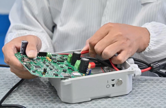
3.3 Stencil Customization and Solder Paste Printing Control for CM4 Characteristics
Solder paste printing is the stage of the SMT process that most significantly impacts soldering quality; industry data indicates that over 70% of SMT soldering defects stem from poor solder paste printing.
Given the high-density nature of the CM4 expansion board, the stencil and printing processes require specialized customization. Instead of using standard uniform aperture scaling, differentiated aperture designs are employed based on component packaging: for 0201 micro-resistors and capacitors, reduced-size apertures are used to prevent solder bridging caused by excessive paste; for CM4 board-to-board connector pins, “recessed” apertures (determined during the DFM phase) are used to maximize the spacing between solder deposits on adjacent pins while ensuring sufficient solder volume; and for the large thermal pads of power chips, grid-pattern apertures are used to ensure soldering reliability while preventing excessive solder paste overflow.
Furthermore, stencil thickness is precisely calibrated to the component density of the CM4 expansion board: 0.12mm stencils are used for standard-density boards, while 0.1mm stencils are used for ultra-high-density boards, ensuring precise control over the solder paste volume for every pad. The solder paste printing stage is fully equipped with 3D SPI (Solder Paste Inspection) systems. After printing, every board undergoes 100% inspection of solder paste thickness, volume, and area for all pads. Any defects—such as misalignment, insufficient or excessive paste, or bridging—are immediately flagged for board cleaning and re-printing; boards with printing defects are strictly prohibited from proceeding to the placement stage.
During printing, the wiping status of the stencil’s underside is checked hourly, and solder paste is replenished at scheduled intervals to ensure highly consistent printing quality across the entire product batch.
SAC305 lead-free, halogen-free solder paste is used, fully complying with halogen content requirements for high-reliability products. Processes regarding storage, thawing, stirring, and usage duration are strictly controlled according to specifications; expired solder paste is scrapped immediately and never used.
3.4 High-Precision SMT Placement and Specialized Reflow Soldering
The CM4 expansion board features a wide range of component packages—from 01005 micro-components to heavy shielding cans and large connectors—placing high demands on the precision and placement capabilities of SMT equipment. The professional manufacturing team utilizes high-precision, multi-functional placement machines with an accuracy of ±0.025mm, fully meeting the alignment requirements for the CM4’s high-density connectors.
Placement programs are optimized to follow a “small-to-large, light-to-heavy” sequence: micro-resistors and capacitors are placed first, followed by IC chips, and finally large, heavy components like the CM4 connector. This prevents the placement head’s movement from dislodging surrounding micro-components after large components have been mounted. Specific placement pressure settings are established for the CM4 board-to-board connector; insufficient pressure results in poor pin-to-pad contact, while excessive pressure risks damaging the connector’s plastic base. Through iterative testing, placement pressure is maintained within an optimal range to ensure every pin aligns precisely with the center of its corresponding pad.
The reflow soldering stage is critical to ensuring solder quality; generic temperature profiles are strictly unsuitable for soldering CM4 expansion boards. Professional process engineers measure and customize specific reflow soldering profiles based on the component layout and the thermal characteristics of the components with the highest thermal mass, strictly adhering to the IPC-7530 standard.
The heating rate in the preheat zone is controlled at 1–3°C/second to ensure uniform temperature rise across all components, preventing deformation caused by excessive thermal gradients. In the reflow zone, the peak temperature is maintained between 245°C and 255°C, with the liquidus dwell time (time above liquidus) controlled at 60–90 seconds; this ensures complete solder melting for reliable metallurgical bonding while preventing damage to the CM4 connector’s plastic structure and surrounding sensitive components due to excessive heat.
Before the production of each batch, a temperature profiler is used to measure actual board temperatures; mass production begins only after confirming the profile fully meets preset requirements. Oven temperatures are re-verified every four hours during production to ensure the stability of the soldering process for the entire batch.
3.5 Comprehensive Post-Soldering Inspection and Defect Capture
After completing SMT reflow soldering, the CM4 expansion board must pass through a multi-level inspection system to intercept all soldering defects before proceeding to the next stage. First, 100% Automated Optical Inspection (AOI) is performed; high-definition industrial cameras capture images of component placement and soldering status, automatically identifying common visual defects such as missing components, wrong parts, misalignment, tombstoning, cold joints, and solder bridging. All suspicious points are flagged for secondary manual visual inspection to ensure no defects are missed.
For high-density pin components like the CM4 board-to-board connector, X-ray inspection supplements AOI. By penetrating the connector’s metal base, X-rays allow for direct observation of the solder joints beneath; this enables the precise identification of defects—such as cold joints or solder bridging—hidden entirely beneath the connector body, thereby eliminating internal soldering risks that conventional visual inspection cannot detect.
All defective units identified during inspection are routed to a dedicated rework area, where professionally trained technicians perform precision repairs using constant-temperature rework stations. Following repair, the units undergo a comprehensive re-inspection process; only those confirmed to be free of defects are returned to the pool of qualified products. Boards with potential soldering flaws are strictly prohibited from proceeding to the functional testing stage.
IV. In-depth Testing and Reliability Verification of CM4 Expansion Board PCBA: From Basic Functionality to Long-term Stability
Many hardware teams limit their understanding of PCBA testing to the notion that “powering up and lighting up” constitutes a pass; however, for products like CM4 expansion boards intended for long-term field operation, merely powering up is far from sufficient. A comprehensive testing and verification system must not only ensure current functional integrity but also simulate potential issues arising from long-term use and extreme environments, thereby exposing latent reliability defects early on.
4.1 ICT Bed-of-Nails Testing and FCT Comprehensive Functional Inspection
In-Circuit Testing (ICT)—or “bed-of-nails” testing—serves as the baseline electrical performance test for the CM4 expansion board. By using custom probe arrays to contact specific test points on the PCB, it directly measures the electrical parameters of individual components. This method rapidly identifies manufacturing defects such as open circuits, short circuits, incorrect or missing components, and parameter deviations. With a test coverage exceeding 95%, it completes a basic electrical performance screening of the entire board in seconds—far more efficiently than manual measurement.
Following successful ICT, a comprehensive Functional Circuit Test (FCT) is performed. The CM4 core module is installed onto the expansion board, and the assembly is powered up. Technicians test the output voltage and current of every power rail to confirm that voltage deviations remain within the design tolerance of ±2% and that no over-voltage or under-voltage issues exist. Subsequently, the communication functions of each peripheral interface are verified individually—including Gigabit Ethernet connectivity, USB data transfer, MIPI image output, and the I/O status of all ports—ensuring that every functional module on the expansion board operates correctly in conjunction with the CM4 module.
Depending on specific product characteristics, FCT also incorporates targeted tests. For instance, smart gateway products undergo continuous network throughput testing—running at full Gigabit load for extended periods—to ensure no packet loss or disconnections occur at the network interface. Industrial I/O control boards undergo individual testing of relay engagement and release actions to confirm the absolute correctness of control logic across all channels. ### 4.3 Specialized Reliability Testing for CM4 Features
Following basic functional testing, a series of specialized reliability tests targeting the core features of the CM4 expansion board are conducted to verify the product’s long-term stability in advance:
First, power supply ripple and full-load burn-in testing. A simulated load is connected to the CM4 expansion board to operate it at 100% capacity. An oscilloscope is used to measure the power supply ripple at the CM4 core power pins, confirming that peak ripple values remain within design limits and ensuring no system crashes occur due to excessive ripple. Subsequently, the board undergoes continuous full-load operation for 72 hours; system status is monitored throughout, and any abnormal reboots or power losses are recorded to expose potential instabilities in the power circuitry early on.
Second, signal integrity spot-checks. Sample boards are randomly selected from each production batch. High-speed oscilloscopes and vector network analyzers are used to measure parameters such as eye diagram quality and impedance characteristics for high-speed signals (e.g., Gigabit Ethernet, USB 3.0). This confirms that the manufactured signal quality aligns with design expectations and prevents issues such as excessive bit error rates in high-speed signals.
Third, environmental stress screening. Based on the product’s application scenario, targeted tests—including temperature cycling, vibration, and drop tests—are performed. Industrial-grade products undergo ten continuous temperature shock cycles ranging from -40°C to 85°C to simulate extreme temperature fluctuations in outdoor environments.
Automotive-grade products undergo random vibration testing compliant with automotive standards to simulate the continuous vibration experienced during vehicle operation. Following environmental stress testing, a comprehensive functional re-inspection ensures the product operates correctly after exposure to extreme conditions, preventing batch failures after delivery to customers.
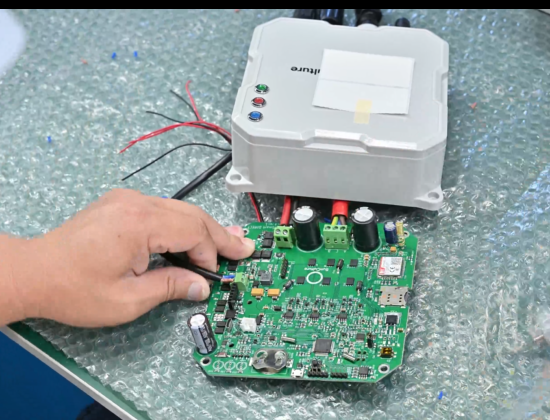
4.4 Conformal Coating and Final Product Inspection
For industrial- and outdoor-grade CM4 expansion boards intended for use in humid, dusty, or salt-spray environments, a conformal coating process is applied after all testing is complete. A transparent conformal coating is evenly sprayed over the board’s surface to form a dense protective film. This film isolates the board from atmospheric moisture, salt, and dust, preventing issues such as electrical leakage, component pin oxidation, and solder joint corrosion during long-term operation.
During the conformal coating process, high-temperature tape is applied in advance to mask areas that do not require coating—such as the contact pins of the CM4 connector and the metal contacts of the USB port—to prevent the coating material from covering these contact surfaces and causing poor connectivity later on.
Once all processing steps are complete, a final comprehensive inspection is performed prior to shipment. This includes checking the board’s appearance for scratches, verifying that solder joints are bright and uniform, and ensuring the absence of residual solder balls or flux residue.
Additionally, all screw holes and mounting holes are checked to ensure they are unobstructed, and all functions undergo a final re-verification. After confirming that all specifications meet the customer’s acceptance criteria, a unique product serial number label is applied, the unit is placed in an anti-static shielding bag for vacuum packaging, and the final product is delivered to the customer. A complete shipment report is provided concurrently, detailing yield data for each batch, key test results, and material batch traceability information, thereby enabling the customer to have full visibility into the manufacturing quality status of the entire batch.
V. Process Standardization and Full-Lifecycle Quality Control for CM4 Expansion Board PCBA Mass Production
Many hardware teams experience smooth sailing during the pilot production phase, only to encounter various quality instabilities once mass production begins. The root cause is often that the manufacturing processes were not fully standardized during the pilot phase, leading to “process drift” across different production batches.
For products like CM4 expansion boards that undergo long-term iteration, PCBA contract manufacturing is not merely a one-off prototyping service; it is a continuous quality control process spanning the entire product lifecycle.
5.1 Process Consolidation and Standardization During the NPI Pilot Phase
Upon completion of the initial CM4 expansion board pilot run, the professional contract manufacturing team generates a comprehensive New Product Introduction (NPI) report. This report compiles and archives all process parameters, issues encountered, and corresponding solutions—including custom stencil designs, reflow profiles, SMT placement programs, AOI inspection parameters, FCT steps, and fixture design blueprints—to establish a fully standardized set of Standard Operating Procedures (SOPs).
For every subsequent mass production run, all production line staff must strictly adhere to these standardized SOPs; unauthorized changes to process parameters are prohibited. Whether switching production lines or changing shifts, process conditions remain identical to those of the initial pilot run. This fundamentally eliminates process variations between batches, ensuring that the manufacturing quality of hundreds or thousands of units matches that of the initial validated samples.
Additionally, a comprehensive Failure Mode and Effects Analysis (FMEA) is conducted during the NPI phase. This process identifies potential manufacturing defects, assesses risk levels, and outlines preventive measures and troubleshooting protocols. Should any anomalies arise during mass production, the team can immediately pinpoint the root cause using these pre-established protocols, resolving issues rapidly to prevent batch-wide defects.
5.2 Quality Traceability and Continuous Iteration Across Multiple Batches
During the production of each CM4 expansion board batch, critical data—including material batch numbers, SMT timestamps, production line station IDs, reflow profile data, AOI inspection results, and FCT test data—are linked to the board’s unique serial number and stored within a comprehensive quality traceability system. Should any board subsequently fail at a client’s site, its complete manufacturing history can be traced back via its serial number. This allows for the precise identification of the failure’s root cause—whether it stems from a material batch issue, process parameter drift, or a design flaw—enabling the rapid formulation of targeted improvements.
Simultaneously, the contract manufacturing team continuously collects yield data for each batch and analyzes the distribution of defects. They then carry out iterative process optimizations focusing on the most prevalent defect types; for instance, if a specific connector model shows a high rate of cold solder joints, the team adjusts the stencil aperture dimensions and reflow soldering temperature profiles to steadily improve soldering yields.
As mass production progresses, the manufacturing yield steadily rises—climbing from approximately 90% during the pilot run to a stable level exceeding 99%—thereby significantly reducing downstream rework and after-sales costs.
5.3 Flexible Manufacturing Adaptation for Long-Tail, Multi-SKU Products
Many product families based on CM4 expansion boards spawn dozens of SKUs with varying configurations, differing only by a few components. To handle these “long-tail” orders, professional contract manufacturing teams implement robust BOM (Bill of Materials) version management systems. Each SKU’s BOM carries a unique version number; before a production line switchover, the system automatically verifies component models and placement locations. Barcode scanning is used to prevent errors, completely eliminating the risk of mixing up materials from different versions.
At the same time, a flexible production scheduling model is employed, allowing small-batch orders for different SKUs to be processed on the same line. Rapid changeover systems enable the quick swapping of placement programs and stencil fixtures. This approach ensures that the production process for every SKU meets all requirements while drastically cutting manufacturing costs for small-batch orders—perfectly aligning with the industry characteristics of edge AI hardware, which often involves high product variety and small-to-medium batch sizes.
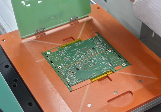
At an Industrial IoT PCBA assembly factory in China
VI. Selection Strategy for CM4 Expansion Board PCBA Contract Manufacturing within Shenzhen’s Hardware Ecosystem
As a premier hub for hardware manufacturing—both domestically and globally—Shenzhen is home to thousands of PCBA contract manufacturers, each with vastly different technical capabilities and service focuses. For hardware teams developing CM4 expansion boards, selecting the right manufacturing partner is far more critical than simply chasing the lowest per-board price. To cut costs early on, many hardware teams opt for small, low-cost contract manufacturers. However, this often results in yields below 60% during the high-density connector soldering stage, with numerous boards suffering from “cold” or defective solder joints. The subsequent costs—in terms of time spent on rework and troubleshooting, as well as wasted materials—far exceed the initial savings on manufacturing fees, and can even delay the product’s time-to-market.
A contract manufacturer truly suited for CM4 expansion boards must possess three core capabilities: First, a comprehensive engineering team capable of handling everything from DFM (Design for Manufacturability) reviews and NPI (New Product Introduction) to full-process testing.
This team needs extensive experience in embedded hardware development and the ability to understand the board’s design logic, rather than simply performing mechanical SMT assembly based on files. Second, the facility must be equipped with specialized inspection tools for high-density boards—such as high-precision 3D SPI and X-ray inspection systems—to detect hidden defects beneath connectors before they become issues. Third, a robust supply chain system is essential to rapidly handle the procurement of CM4-specific components and manage the switch to alternative parts, ensuring production does not stall due to a shortage of a single component.
For hardware teams in Shenzhen, choosing a local PCBA manufacturer for CM4 expansion boards offers a unique geographical advantage: the turnaround from design file submission to receiving the first prototype can be as fast as 3–5 days. If manufacturing issues arise, engineers can drive directly to the factory floor to communicate face-to-face with process engineers, allowing problems to be identified and resolved on the same day—a level of collaborative efficiency that remote manufacturers simply cannot match.
Conclusion
PCBA manufacturing for CM4 expansion boards is by no means a simple, low-barrier process; rather, it is a systematic undertaking that deeply integrates hardware design expertise, precision manufacturing processes, supply chain management capabilities, and reliability verification systems. Many hardware teams pour all their energy into circuit design and software development while overlooking the complexities of the manufacturing process.
This often results in a product with excellent design failing to achieve stable mass production in a timely manner. A truly mature CM4 expansion board is the result of close collaboration between design and manufacturing: manufacturing feasibility is considered early in the design phase, while professional manufacturing capabilities ensure that all design specifications are fully realized during production. Through process stabilization during the New Product Introduction (NPI) phase and continuous iteration across multiple batches, a mass-production yield of over 99% is ultimately achieved. Only by mastering every manufacturing detail—from design adaptation to mass-production delivery—can CM4-based edge intelligence products transition from laboratory prototypes to stable, large-scale field deployments, thereby fully realizing their technical value in applications such as the Industrial Internet of Things (IIoT), smart gateways, and embedded control systems.