
Inverter Control Board PCBA Factory: From Precision Signal Control to Reliable Manufacturing.
The core function of an inverter is to convert and regulate electrical energy according to specific requirements. Within this process, the control board PCBA plays a critical role: it must capture real-time operational parameters—such as voltage, current, and temperature—generate PWM drive signals based on control algorithms, and coordinate power components to ensure stable energy conversion.
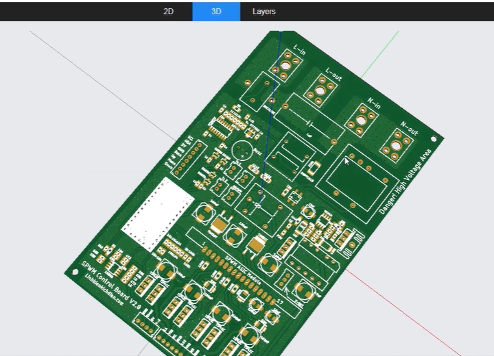
Compared to standard industrial control boards, inverter control boards typically operate in environments characterized by high-frequency switching, high voltages, and intense electromagnetic interference (EMI). Even a minor deviation in sampling, an anomaly in a drive signal, or an improper grounding design can compromise the efficiency and operational stability of the entire system.
Therefore, when selecting a PCBA manufacturer for inverter control boards, one should look beyond mere placement precision. It is essential to evaluate the manufacturer’s depth of understanding regarding power electronics, as well as their capabilities in process control and testing.
The primary manufacturing challenge for inverter control boards lies in signal reliability.
Manufacturing an inverter control board involves more than simply mounting components onto a PCB. It requires the integration of digital control, analog sampling, power driving, and communication interfaces—all of which share complex electrical interdependencies.
Analog Sampling and Control Precision
Circuits responsible for sampling voltage and current directly influence the decisions made by control algorithms. The layout of sampling resistors, operational amplifiers, filtering networks, and ADC inputs must carefully account for noise coupling, signal return paths, and component parameter tolerances. In scenarios involving high currents and rapid fluctuations, the stability of the sampled signals is directly linked to the system’s control response.
Gate Driving and Isolation Design
Power switching devices, such as IGBTs and MOSFETs, require precisely matched drive signals provided by dedicated drive circuitry. Drive loops must be kept as short as possible to minimize parasitic inductance, while system architecture dictates the requirements for isolation spacing, drive power supplies, and protection signaling. For high-voltage applications, factors such as electrical clearance, creepage distance, and the placement of isolation components cannot be managed using standard PCB design practices.
Electromagnetic Interference (EMI) and Grounding Management
High-frequency noise generated by power switching devices can couple into control circuits via power lines, ground traces, or parasitic capacitance. Before manufacturing a control board, it is essential to distinguish between power circuits, drive circuits, and sensitive signal areas based on the PCB layout. This ensures that high-noise traces do not cross through sampling or communication zones. For a PCBA manufacturing facility, understanding these design boundaries helps in identifying potential issues early during the production and engineering review stages.
From PCB Design to SMT Assembly: Process Details Determine Consistency
Inverter control boards typically incorporate MCUs, DSPs, isolated gate drivers, precision sampling components, communication interfaces, and various power management elements. Different components have specific requirements regarding soldering temperatures, placement accuracy, and solder joint quality.
During the manufacturing process, particular attention should be paid to the following aspects:
PCB and Pad Quality: Verify the board material, copper thickness, surface finish, solder mask openings, and pad dimensions to ensure they align with component footprints and the chosen soldering process.
SMT Placement: For fine-pitch ICs, QFNs, and other high-density packages, strictly control solder paste printing, placement offset, and reflow soldering temperature profiles.
Through-hole and Large Components: For connectors, transformers, inductors, and high-power components, focus on solder joint fill, mechanical securing, and the thermal capacity required for soldering.
Cleaning and Protection: Based on operating voltage, ambient humidity, and product application, evaluate flux residue, cleaning requirements, and conformal coating strategies to prevent contaminants from affecting high-impedance or high-voltage areas.
It is important to note that conformal coating is not a substitute for proper electrical clearance design. The coating material, coverage area, and curing conditions must all be validated against product specifications.
Testing Inverter Control Boards: Beyond Visual Inspection
For products of this nature, Automated Optical Inspection (AOI) can only detect a portion of soldering and placement defects; it cannot confirm whether the control board will deliver reliable performance under actual operating conditions.
A comprehensive quality validation strategy should be structured across multiple levels:
Level 1: Manufacturing Quality Inspection
Utilize Solder Paste Inspection (SPI), AOI, X-ray (where applicable), and solder joint inspection to identify issues such as solder paste printing deviations, component misalignment, cold/dry joints, solder bridges, and defects in hidden solder joints.
Level 2: Electrical and Programming Verification
Using In-Circuit Testing (ICT) or flying-probe testing, applicable electrical nodes are inspected to verify power rails, critical resistance values, the absence of short circuits, communication interfaces, and the status of controller firmware programming.
Level 3: Functional and Load Verification
Utilizing a complete system setup or a dedicated test platform, the control board is evaluated for power-on sequencing, PWM output, sampling feedback, overcurrent and overvoltage protection, temperature sensing, and communication functionality. Where conditions permit, control response and fault-protection logic should also be validated using simulated loads or actual power systems.
Truly valuable testing goes beyond simply recording whether a product powers on; it confirms that critical control functions operate exactly as designed.
Different Inverter Applications Impose Distinct Requirements on PCBA Manufacturing
While photovoltaic (PV) inverters, energy storage inverters, industrial variable-frequency drives (VFDs), and automotive power conversion systems all involve the conversion of DC to AC power, they differ significantly in terms of operating environments, control strategies, and reliability requirements.
For instance, PV inverter control boards require a focus on temperature fluctuations during long-term operation, sampling accuracy, and communication stability.
Energy storage inverters must balance battery management interfaces, power regulation, and protection logic. Industrial VFDs, meanwhile, prioritize motor control response, electromagnetic interference (EMI) immunity, and resilience to harsh field operating environments.
Consequently, a PCBA manufacturer cannot rely on a standardized set of production parameters for every project. Board architecture, component selection, soldering processes, and test protocols must all be evaluated based on the specific application.
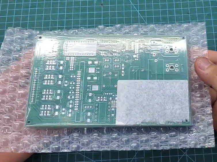
KingTop Technology: PCB and PCBA Manufacturing Support for Power Electronics
KingTop Technology specializes in PCB fabrication and PCB assembly, providing manufacturing support for projects in industrial control, power electronics, and other electronic equipment sectors.
For inverter control board projects, KingTop Technology offers comprehensive services—including PCB fabrication, electronic component sourcing, SMT (Surface Mount Technology) placement, DIP (Dual In-line Package) insertion, final assembly, and quality inspection. Production feasibility is assessed based on the Gerber files, Bill of Materials (BOM), coordinate files, and assembly specifications provided by the client.
For boards featuring precision sampling, isolated gate driving, or high-density control circuitry, a DFM (Design for Manufacturing) review prior to production is particularly critical. By examining component footprint compatibility, pad design, component spacing, manufacturability, and test interfaces, potential issues that could impact mass production can be identified at an early stage.
At KingTop Technology, the focus extends beyond the mere completion of PCB assembly; we ensure that the manufacturing process aligns with the product’s design objectives. This helps clients mitigate manufacturing risks during the engineering transition and establishes a stable foundation for subsequent mass production.
Conclusion
The value of an inverter control board PCBA lies not in the number of components it contains, but in the ability of its complex circuitry to execute control commands accurately and reliably over the long term.
For a PCBA manufacturer, the true technical threshold is defined by a comprehensive understanding of signal integrity, power drive, electromagnetic compatibility (EMC), soldering processes, and functional verification. Only by integrating engineering assessment, precision assembly, and targeted testing can one provide a more reliable manufacturing foundation for inverter control boards.