
With the rapid evolution of intelligent cockpits, Advanced Driver Assistance Systems (ADAS), and centralized electronic/electrical (E/E) architectures, automotive electronics are accelerating toward a new era defined by high data throughput, multi-sensor fusion, and high-density integration.
As a professional Electronics Manufacturing Services (EMS) provider deeply rooted in high-end electronics manufacturing and automotive-grade assembly, KingTop Technology recognizes that High-Density Interconnect (HDI) printed circuit board assemblies (PCBAs) have become the core “nervous system” of modern intelligent vehicles.
Unlike consumer electronics, automotive-grade HDI systems must maintain absolute reliability and zero-defect operation within extremely harsh environments. This includes enduring severe temperature cycling, intense mechanical vibration, humidity, electromagnetic interference (EMI), and meeting a long-term design lifespan exceeding 15 years.
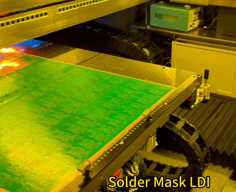
Leveraging a 10,000-square-meter Class 100,000 cleanroom, 10 high-precision fully automated SMT production lines, and a seasoned engineering team of over 260 professionals, KingTop Technology has developed this technical white paper. It provides a systematic analysis of core process standards, quality control systems, and advanced manufacturing specifications for automotive HDI PCB assembly—offering robust “smart manufacturing” support to innovators in the global automotive electronics sector.
I. Core Technical Challenges and Automotive-Grade Standards for HDI PCB Assembly in Automotive Systems
Environmental Adaptability and Reliability Standards for Automotive-Grade Electronics Manufacturing
Automotive electronic devices operate in environments far more demanding than those encountered by standard industrial or consumer electronics. Within engine compartments, domain controllers, or chassis control systems, operating temperature ranges often span from -40°C to +125°C—or even higher—with some critical locations subjected to extreme thermal shock and high-frequency vibration.
Consequently, the assembly design of automotive HDI boards must strictly adhere to the IATF 16949 automotive quality management system. Furthermore, the selection and validation of all passive and active components must comply with AEC-Q200 and AEC-Q100 standards.
Furthermore, soldering and assembly processes must comply with the IPC-A-610 Class 3 acceptance standard (the classification for aerospace and advanced automotive electronics). To withstand thermomechanical stress induced by alternating thermal conditions, the PCB substrate, solder mask, underfill, and surface finish must exhibit a high degree of coefficient of thermal expansion (CTE) matching. This is critical to preventing failures such as microvia fractures, solder joint fatigue cracking, or delamination resulting from long-term thermal cycling.
Structural Characteristics of High-Density Interconnect (HDI) in Automotive Multilayer PCBs and Microvia Technology
Modern intelligent cockpit SoCs, high-performance AI processors, and automotive communication modules feature extremely high pin densities and ultra-fine pitches. Traditional through-hole PCBs are no longer capable of meeting the requirements for routing density and signal integrity in these applications.
Automotive HDI boards frequently utilize 1+N+1, 2+N+2, or even “Any-Layer” interconnect structures. Microvias are typically formed using laser direct drilling, with diameters controlled between 75μm and 100μm.
In assembly design, the “via-in-pad” technique—involving the electroplating and filling of microvias—is of paramount importance. If a via is not fully filled or contains microscopic voids, the expansion of trapped chemical residues or air during high-temperature reflow soldering (or subsequent thermal shock in automotive environments) can easily cause the copper layer on the via wall to rupture. Consequently, our facility employs advanced pulse electroplating and full-panel via-filling processes. This ensures a uniform copper thickness within the microvias and a level of planarity that exceeds IPC standards, fundamentally guaranteeing both the electrical connectivity and the mechanical structural integrity of the high-density interconnects.
Design Considerations for Signal Integrity (SI) and Power Integrity (PI) in High-Frequency, High-Speed Automotive Connected Systems
With the widespread adoption of Automotive Ethernet, gigabit GMSL (Gigabit Multimedia Serial Link) camera serial links, high-speed PCIe buses, and 5G/V2X wireless communications, signal frequencies and edge rates on automotive HDI (High-Density Interconnect) PCBs have increased significantly.
Signal Integrity (SI) and Power Integrity (PI) have emerged as critical bottlenecks determining system stability. During the assembly and stack-up design phases, tolerances for differential impedance (typically 85Ω or 100Ω) and single-ended impedance (typically 50Ω) must be strictly controlled within a range of ±5%.
Substrate selection must prioritize high-frequency, high-speed copper-clad laminates (such as Megtron 6/7 or equivalent materials) that feature a low dielectric constant (Dk) and a low dissipation factor (Df) to minimize signal attenuation and dispersion. Furthermore, in the design of the Power Distribution Network (PDN), high-frequency noise and ground bounce are effectively suppressed by optimizing the placement of decoupling capacitors, shortening current loops, and increasing capacitive coupling between power and ground planes. This ensures voltage stability for multi-core SoCs during transient, high-current switching events.

II. Design Specifications and Stack-up Optimization for Automotive HDI PCBs
Stack-up Design (Build-up Lamination) and Impedance Control Strategies for Automotive HDI PCBs
A well-engineered, rational stack-up structure is the cornerstone for ensuring Electromagnetic Compatibility (EMC) and signal transmission quality in automotive HDI PCBs. During the stack-up design process, a symmetrical lamination principle is strictly followed to prevent PCB warping or deformation during multi-stage thermal pressing and soldering processes.
Typically, this involves the use of Resin-Coated Copper (RCC) or core-based laminates, combined with a multi-stage laser drilling and lamination process. For multi-layer high-speed digital boards, the top and sub-surface layers are utilized for routing sensitive clock signals and high-speed differential pairs, with adjacent, continuous reference planes (GND/PWR) providing excellent return paths.
Regarding the selection of dielectric thickness, the resin content of the prepreg and the specific glass fabric style (e.g., 106, 1080, or 2116) are precisely calculated to mitigate the “fiber weave effect,” which can otherwise cause impedance fluctuations in high-frequency, high-speed microstrip lines. Rigorous impedance design and simulation are not only strictly controlled during the PCB fabrication process but are also validated through a closed-loop verification system—spanning the Design for Manufacturing (DFM) phase through to bare-board testing prior to assembly.
Laser-drilled micro-vias, “via-in-pad” (filled via) structures, and thermal stress relief
In highly integrated automotive PCBs, “via-in-pad” designs are widely employed for high-density BGA fan-outs to conserve valuable routing space. However, if these vias are not filled with resin and capped with a plated copper layer, solder may flow into the vias during surface-mount technology (SMT) assembly. This can lead to insufficient solder volume, excessive voiding, or even “cold” (non-wetting) solder joints.
Consequently, our design and manufacturing specifications mandate a “resin-filled and plated-over” (plated-over filled via) process, ensuring that the surface flatness of the pads is controlled within the micron range. Furthermore, to alleviate thermal stress—such as that caused by engine vibrations or extreme temperature fluctuations—we incorporate “hatched” (grid-patterned) copper in large copper-pour areas. We also utilize “thermal relief” connections to minimize heat dissipation during soldering, ensuring that every SMT joint develops a uniform and robust intermetallic alloy layer.
Golden Rules for Layout and Routing of HDI Boards for Intelligent Cockpits and ADAS Domain Controllers
Automotive domain controllers feature an extremely high level of integration. A single HDI board often houses high-heat, high-compute AI chips, high-power power management ICs (PMICs), sensitive RF transceiver front-ends, and precision analog sensor interfaces.
During the layout design phase, we strictly adhere to the principle of zone isolation: digital high-frequency sections, analog small-signal sections, power conversion sections, and power drive sections must be physically separated to prevent digital switching noise from coupling into the analog/RF domains. For high-heat components like SoCs and power ICs, we design large-area thermal pads and utilize arrays of thermal vias to efficiently conduct heat to the underlying thermal backplane or enclosure.
Furthermore, high-current traces must feature sufficient copper thickness and trace width to prevent excessive voltage drops or temperature rises. Sensitive communication buses—such as CAN FD, LIN, and Ethernet differential pairs—must be routed away from high-power inductors and transformers. These traces must also be length-matched and surrounded by ground shielding to ensure optimal electromagnetic isolation.
III. Surface Mount Technology (SMT) and Advanced Assembly Process Control
Solder Paste Printing and SPI (Solder Paste Inspection) Precision Control for Ultra-Fine Pitch Components
Automotive HDI boards are densely populated with ultra-fine pitch components, including QFPs, BGAs and CSPs with 0.4mm/0.3mm pin pitches, and flip chips. Solder paste printing serves as the critical first checkpoint that determines the yield of the SMT assembly process.
We employ high-precision, fully automated vision-aligned printing machines equipped with nano-coated stencils and laser-cut apertures to ensure a 100% solder paste release rate. Regarding process parameters, we precisely calibrate squeegee pressure, print speed, and separation speed based on the specific dimensions of the component pads. Following the printing process, the entire production line is equipped with high-precision 3D Solder Paste Inspection (SPI) systems. These perform 100% in-line 3D inspection of every solder pad, measuring the volume, area, height, and offset of the deposited solder paste. The system detects and flags any issues—such as insufficient or excessive solder, bridging, or misalignment—in real time, effectively preventing downstream soldering defects caused by solder paste irregularities at the source.
High-Precision Placement of Odd-Form Components, BGAs, PoP (Package-on-Package), and Flip Chips
Automotive electronics encompass not only standard chip-type resistors and capacitors but also a wide array of heavy, odd-form, and custom-designed components—including connectors, transformers, shielding cans, and complex PoP (stacked package) chips.
We utilize a fleet of advanced, high-speed, multifunctional modular placement machines equipped with high-resolution vision alignment systems. These systems enable sub-micron-level precision alignment for BGA ball arrays and ultra-fine-pitch components.
For complex, irregularly shaped connectors, we employ custom-designed nozzles and placement heads with force-feedback control; this ensures that downward pressure is precisely regulated, preventing mechanical damage to delicate HDI ceramic or multi-layer resin-based substrates.
For moisture-sensitive ICs (MSL levels 3 through 5), we enforce strict pre-placement baking and vacuum-sealed moisture protection protocols. Furthermore, all placement operations are conducted within a strictly controlled, constant-temperature and constant-humidity cleanroom environment.
Reflow Profile Optimization and Lead-Free Soldering Quality Control
Automotive HDI boards present significant reflow soldering challenges due to their high number of copper layers, substantial thickness, and highly uneven thermal mass distribution across components. To address this, we utilize large-scale, full-convection reflow ovens featuring 10 or more heating zones.
These ovens operate under a nitrogen (N₂) atmosphere, with oxygen concentration strictly maintained below 50 ppm to minimize metal oxidation at high temperatures and enhance wetting performance. For each automotive-grade HDI board, process engineers conduct rigorous reflow profiling using multi-channel thermocouple data loggers to precisely establish temperature gradients across the preheat, soak, reflow, and cooling zones.
Key parameters—specifically peak temperature and Time Above Liquidus (TAL)—are meticulously optimized. This ensures that solder joints beneath components with high thermal mass melt thoroughly, while simultaneously preventing smaller components from suffering heat-related damage or the PCB substrate from undergoing thermal delamination. Furthermore, by strictly controlling the cooling rate, a dense intermetallic compound (IMC) layer is formed, granting the solder joints exceptional mechanical resistance to fatigue and vibration.
IV. Quality Inspection, Reliability Verification, and Failure Analysis for Automotive-Grade HDI Board Assembly
Application of 3D AOI and 3D X-Ray (AXI) for Non-Destructive Inspection of Hidden Solder Joints
In the assembly of automotive HDI boards, many solder joints—associated with high-density BGA, QFN, and LGA components, as well as double-sided mixed-technology assemblies—are completely concealed beneath the components themselves, rendering them invisible to traditional 2D Automated Optical Inspection (AOI). To address this, we have implemented a dual-layered, non-destructive inspection strategy: 3D AOI combined with 3D Automated X-Ray Inspection (AXI).
High-resolution 3D AOI performs rapid, comprehensive screening of all surface-mounted components to detect issues such as incorrect polarity, misalignment, tilted components, or “tombstoning.” Meanwhile, advanced 3D X-Ray (AXI) tomography systems conduct 3D cross-sectional scanning to evaluate the quality of BGA solder ball arrays. These AXI systems utilize intelligent AI algorithms to automatically analyze the voiding ratio within BGA solder joints.
Adhering to the highest automotive-grade standards, we strictly limit the area of any single void within a BGA solder joint to less than 15%, and the total void area to less than 25%. This rigorous control effectively eliminates potential failure risks—such as “dry” (non-wetted) joints, solder bridging, cold joints, or excessive voiding—that could otherwise compromise reliability.
Automotive-Grade Environmental Stress Screening (ESS): Thermal Shock, Vibration, and Temperature-Humidity-Bias (THB) Testing
To ensure that the products delivered to our clients possess the exceptional reliability required to withstand a decade of harsh operating conditions, we conduct rigorous Environmental Stress Screening (ESS) and reliability verification testing—either prior to mass production or in accordance with specific customer requirements.
Our testing regimen includes extreme temperature cycling (ranging from -55°C to +125°C, involving thousands of rapid transitions), random vibration and mechanical shock testing (simulating the high-energy, full-spectrum vibrations experienced by vehicles on rough terrain), Temperature-Humidity-Bias (THB) testing (accelerated aging at 85°C/85% RH under electrical bias), and salt spray corrosion testing.
By subjecting our products to these grueling environmental extremes, we identify and eliminate units prone to early-life failure. This ensures that every automotive HDI board assembly leaving our facility is built to remain robust and durable throughout the entire vehicle lifecycle.
Electrical Performance Testing in Demanding Environments (ICT, FCT, and Boundary Scan) and Failure Prevention Mechanisms
Pre-shipment electrical performance verification serves as the final safeguard in achieving our “zero-defect” quality objective. We develop customized testing solutions for every automotive project, including In-Circuit Testing (ICT) and Functional Testing (FCT).
ICT precisely detects open circuits, short circuits, resistance values, capacitance, and diode characteristics for individual components. FCT utilizes test benches that closely simulate real-world automotive operating environments; by applying operational voltage to the HDI board assemblies and emulating CAN and LIN bus communications, we perform 100% automated, full-functional testing—covering all I/O ports, sensor signal acquisition, power conversion efficiency, and logic control functions.
For digital chips featuring complex internal scan chains, we employ JTAG Boundary Scan technology. This allows for in-depth verification of interconnect integrity for internal chip pins without the need for physical probe contact, establishing a comprehensive error-proofing and failure-prevention framework.
V. Manufacturing Collaboration: End-to-End Assurance from DFM (Design for Manufacturability) to Mass Production Delivery
In-depth DFM (Design for Manufacturability) Evaluation System for Automotive HDI PCBs
High-quality automotive electronics manufacturing begins with rigorous front-end engineering design. Upon receiving design documentation from a client, our experienced senior DFM engineering team immediately intervenes to conduct a comprehensive, in-depth review of manufacturability and assemblability.
This review goes beyond standard parameters—such as drill-to-pad ratios, solder mask web widths, and stencil aperture design—to focus on critical aspects specific to automotive HDI PCBs. These include copper thickness balancing, the prevention of “acid traps,” thermal balance design, panelization efficiency optimization, and the strategic placement of test points.
By identifying and rectifying potential manufacturing defects early in the design phase, we help clients avoid repetitive revisions during the prototyping stage. This significantly shortens the New Product Introduction (NPI) cycle, ensuring a seamless transition from design blueprints to high-yield, mass-produced products.
Supply Chain Traceability, Component Control, and ESD-Controlled Manufacturing Environment
The automotive supply chain imposes stringent requirements on the quality and traceability of electronic components. We have established a robust supply chain management system; all materials are sourced exclusively from original manufacturers or authorized Tier-1 distributors, effectively eliminating the risk of counterfeit or substandard components. Every incoming batch of materials undergoes rigorous Incoming Quality Control (IQC) and random X-ray inspection.
During the manufacturing process, each PCB is assigned a unique laser-etched QR code (barcode). This enables full-lifecycle digital traceability—from raw material batches and specific SMT placement machines to reflow oven temperature profiles and final test results.
Furthermore, our SMT and assembly facilities operate under Class 10,000 cleanroom standards, with strictly controlled temperature and humidity levels. All personnel are required to wear anti-static gear, and our facility features comprehensive grounding and real-time electrostatic monitoring, ensuring that Electrostatic Discharge (ESD) sensitive components receive the highest level of protection.
Summary
As a technology-driven manufacturer and exporter of PCBs and PCBAs with global service capabilities, KingTop Technology operates a 10,000-square-meter, Class 100,000 (ISO 8) cleanroom facility, equipped with 10 high-precision, fully automated SMT production lines and supported by a team of over 260 seasoned engineering and technical professionals.
Guided by a steadfast commitment to craftsmanship and continuous improvement, we consistently refine our micro-blind via assembly processes, optimize advanced SMT manufacturing workflows, and uphold a rigorous, automotive-grade quality assurance system.
We look forward to forging deep partnerships with Tier 1 automotive electronics suppliers, OEMs, and innovative technology enterprises worldwide. By leveraging our cutting-edge intelligent manufacturing prowess and our pledge to zero-defect quality, we aim to empower the high-quality advancement of the global automotive electronics industry—driving toward a new era of mobility that is smarter, safer, and more reliable.