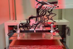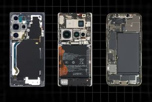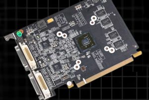

Automotive HDI (High-Density Interconnect) PCB assembly and manufacturing is a critical process within the automotive electronics production ecosystem.
It is widely applied in products such as intelligent cockpit systems, Advanced Driver Assistance Systems (ADAS), automotive cameras, millimeter-wave radar, body control modules, powertrain control systems, and in-vehicle communication equipment.
Compared to standard PCB assembly, automotive HDI boards are characterized by higher circuit density, finer pad pitch, complex micro-via structures, higher component integration, and stringent requirements for signal integrity.
The assembly and manufacturing process requires not only ensuring the quality of electronic component soldering but also strictly controlling factors such as solder paste printing on tiny pads, precision component placement, reflow soldering temperature profiles, the reliability of BGA (Ball Grid Array) solder joints, and the overall electrical performance of the board.
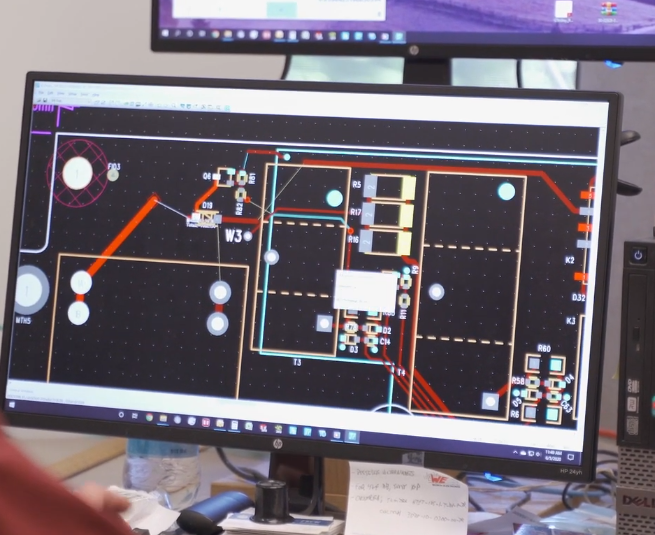
This article focuses on the automotive HDI PCB assembly process, covering incoming material inspection, solder paste printing, Solder Paste Inspection (SPI), SMT (Surface Mount Technology) placement, reflow soldering, Automated Optical Inspection (AOI), X-ray inspection, DIP (Dual In-line Package) and manual/secondary soldering, cleaning, conformal coating, functional testing, and final product inspection. It does not cover the fabrication of the bare PCB itself (i.e., circuit patterning, lamination, drilling, or electroplating).
I. The Complete Process of Automotive HDI PCB Assembly and Manufacturing
Incoming Material Inspection (IQC) for PCBs and Electronic Components
Incoming material inspection is the first quality control step in the assembly and manufacturing of automotive HDI boards; it directly impacts subsequent soldering quality and overall product reliability.
Bare PCB Inspection:
Verify that the PCB model, revision, thickness, dimensions, and panelization layout conform to the Bill of Materials (BOM) and engineering documentation.
Confirm that the surface finish (e.g., ENIG, immersion silver, OSP, etc.) meets product specifications.
Inspect pads for signs of oxidation, contamination, scratches, discoloration, or other surface anomalies.
Check the board for delamination, blistering, warping, physical damage, or misregistration of the solder mask.
Specifically, examine areas containing HDI micro-vias, blind vias, and buried vias for any irregularities that could compromise the assembly process. Verify the solderability, dimensions, and required flatness of the PCBs.
Electronic Component Inspection:
Verify the Bill of Materials (BOM), part numbers, specifications, package types, and manufacturer information.
Inspect the physical condition of components such as ICs, BGAs, QFNs, CSPs, and passive components (e.g., 0402, 0201).
Check the Moisture Sensitivity Level (MSL) rating, vacuum packaging, desiccant, and humidity indicator cards.
For moisture-sensitive components requiring baking, follow the procedures outlined in IPC/JEDEC J-STD-033 and the component manufacturer’s specifications.
For critical automotive-grade components, verify batch numbers, traceability information, and supplier quality documentation.
Process Control Focus: Establish a traceability system for PCB and component batches to prevent the use of incorrect or mixed materials, as well as the entry of moisture-affected or non-conforming materials into the production line.
PCB Loading and Pre-Production Preparation
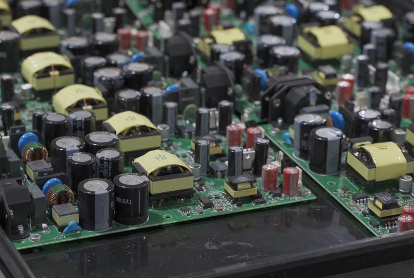
Develop a comprehensive production preparation plan based on the structure of the automotive HDI (High-Density Interconnect) boards, panelization layout, and SMT equipment requirements.
Key tasks include:
Verify production work orders, BOMs, Gerber files, coordinate files, and stencil specifications.
Confirm the PCB panel orientation, fiducial marks, and positioning methods.
Select appropriate carriers and support fixtures based on the PCB dimensions and board layout.
Review SMT equipment programs, placement coordinates, and component footprint libraries.
Ensure compatibility between the stencil thickness, aperture dimensions, and pad design.
Perform necessary PCB baking and pre-treatment, following guidelines specific to the board material, surface finish, and supplier requirements.
For thin HDI boards, multi-layer high-density boards, and PCBs with localized high-density component placement, prioritize board support to prevent warping or bowing during the printing and component placement processes.
Solder Paste Printing
Solder paste printing is a core process in SMT assembly; it directly influences solder joint formation and the occurrence of defects such as short circuits, “cold” (open) joints, and overall solder joint reliability.
Key process steps:
Install the appropriate stencil based on the PCB pad layout.
Verify the solder paste batch, expiration date, storage temperature, and “thawing” (warm-up) status. Stir the solder paste in accordance with process requirements.
Adjust the squeegee pressure, speed, and angle, as well as the stencil release parameters.
Precisely transfer the solder paste onto the PCB pads through the stencil apertures.
Inspect the solder paste coverage, thickness, and shape after printing.
Key Process Controls:
Optimize stencil aperture design for ultra-small packages such as 0201 and 01005.
Ensure consistent solder paste volume for components like BGA, QFN, and LGA.
Control the gap (contact clearance) between the stencil and the PCB.
Prevent issues such as solder paste offset, insufficient or excessive solder, bridging, and slump.
Regulate the printing environment’s temperature and humidity, as well as the solder paste’s usage duration, in accordance with its technical specifications.
Automotive HDI boards feature fine pad spacing, requiring high-precision solder paste printing. Stencil parameters must be determined through rigorous process validation; standard printing conditions used for conventional PCBs cannot simply be applied here.
Solder Paste Inspection (SPI)
SPI (Solder Paste Inspection) utilizes 2D or 3D vision technology to evaluate the quality of the solder paste printing process.
Key Inspection Criteria:
Solder paste height and volume.
Solder paste coverage area.
Solder paste printing offset.
Missing or insufficient solder paste.
Solder bridging (unintended connections between adjacent pads).
Print shape and consistency.
For automotive HDI boards, SPI is used not only to identify printing defects but also to correlate inspection data with subsequent AOI (Automated Optical Inspection), X-ray results, and soldering defect records, thereby establishing a feedback loop for process parameter optimization.
SMT Precision Placement (Pick & Place)
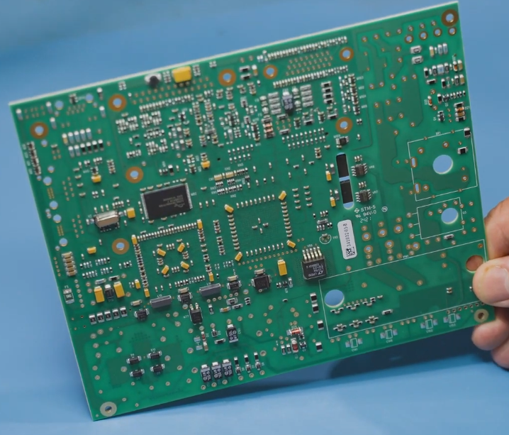
SMT placement is the process of accurately mounting electronic components onto their designated pad locations on a PCB, based on design coordinates.
Typical Components for Placement:
Miniature chip components (e.g., 0201, 0402, 0603).
High-density packaged devices (e.g., BGA, CSP, QFN, LGA).
MCUs, CPUs, memory modules, and power management ICs.
RF components, sensors, and automotive communication modules.
Connectors, crystal oscillators, and other specialized packages. Key Process Control Points:
Precisely calibrate the pick-and-place machine’s vision system and the PCB fiducial marks.
Control nozzle selection, pick-up pressure, and placement height.
Optimize component placement angle, center offset, and rotational accuracy.
Prevent defects such as “tombstoning,” misalignment, missing components, incorrect components, and reversed orientation.
For BGAs and fine-pitch ICs, focus on controlling placement position and coplanarity.
Optimize placement pressure based on component weight, package type, and solder paste characteristics.
Automotive HDI (High-Density Interconnect) boards typically integrate a large number of miniature components; the placement process must prioritize positional accuracy and batch-to-batch consistency.
Reflow Soldering
Reflow soldering is a critical process that uses controlled heating to melt the solder within the solder paste, forming reliable solder joints.
Typical temperature zones include:
Preheat Zone: Gradually raises the temperature of the PCB and components to minimize thermal shock.
Soak Zone: Facilitates flux activation and improves wetting conditions on the surfaces of pads and component leads.
Reflow Zone: Heats the solder above its liquidus temperature to complete the soldering process.
Cooling Zone: Controls the cooling rate to ensure the formation of a stable metallic microstructure within the solder joints.
Key Process Controls:
Determine the peak temperature based on the solder paste supplier’s specifications.
Control the Time Above Liquidus (TAL).
Regulate the heating rate, soak duration, and cooling rate.
Verify the actual PCB temperature profile using thermocouples.
Analyze temperature uniformity, especially for BGAs, QFNs, and large-sized components.
Monitor variations in PCB thermal capacity and localized temperature deviations.
For automotive HDI boards, it is particularly important to prevent BGA voids, solder joint cracking, cold joints, “dry” (non-wetting) joints, component misalignment, and thermal deformation of the PCB.
Note: Reflow soldering parameters should not be fixed or uniform; the process window must be established by considering the solder paste alloy system, the heat resistance ratings of the components, the PCB’s thermal capacity, and actual temperature measurement results.
Automated Optical Inspection (AOI)
AOI utilizes optical imaging and image-processing algorithms to automatically inspect PCBs after the SMT soldering process.
Primary inspection targets:
Missing components, incorrect components, and reversed orientation. Component displacement or abnormal rotation.
Insufficient solder, solder bridging, and other evident soldering anomalies.
“Tombstoning” (components standing on end) and physical damage to components.
Incorrect polarity and misplacement of components.
For automotive HDI (High-Density Interconnect) assemblies, AOI (Automated Optical Inspection) programs should be configured based on specific product design and process requirements to minimize false-call rates while ensuring that critical defects are not overlooked.
X-Ray Inspection (Critical Process)
Because the solder joints of components such as BGAs (Ball Grid Arrays) and CSPs (Chip Scale Packages) are located beneath the component body, they cannot be inspected by standard AOI; therefore, X-Ray inspection is required.
Key inspection criteria include:
Void ratio and distribution within BGA solder joints.
Missing solder balls, bridging, and abnormal solder ball shapes.
Solder joint displacement and uneven soldering.
Abnormal connections at hidden solder joints.
Soldering status of the thermal pad (bottom pad) on QFN (Quad Flat No-lead) components.
For automotive controllers, ADAS (Advanced Driver Assistance Systems) units, and other high-reliability electronic modules, X-Ray inspection strategies—ranging from sampling to 100% inspection—should be established based on the product’s risk profile.
It should be noted that while X-Ray inspection can identify certain internal soldering defects, it cannot, on its own, guarantee the long-term mechanical reliability of a solder joint; this must be verified through process validation and reliability testing.
Through-Hole Component Insertion and Selective Soldering
Automotive HDI boards that utilize both SMT (Surface Mount Technology) and THT (Through-Hole Technology) require the insertion of through-hole components followed by a soldering process.
Key process steps include:
Manual or automated component insertion.
Verification of component orientation and placement.
Control of component lead length.
Selective wave soldering or other appropriate soldering methods.
Necessary manual touch-up soldering and joint refinement.
For high-density HDI boards, selective soldering helps minimize localized thermal impact, preventing unnecessary secondary thermal stress on components already attached via SMT.
Following the soldering of through-hole components, inspections must be performed to check for proper solder wetting, hole filling, bridging, “cold” (or weak) joints, and lead-related defects.
Cleaning and Conformal Coating
Depending on the product’s operating environment and specific customer technical requirements, some automotive HDI assemblies may require cleaning and the application of a conformal coating.
PCB Cleaning:
Removal of soldering residues, flux residues, and other contaminants.
Selection of an appropriate cleaning method based on the type of flux used. Control the concentration and temperature of the cleaning solution, as well as the cleaning duration.
Focus cleaning efforts on the areas surrounding BGAs, connectors, and the undersides of components.
Ensure thorough drying after the cleaning process.
Not all “no-clean” solder pastes require cleaning; however, the use of no-clean materials does not eliminate the risk of ionic contamination. The decision to clean should be based on customer requirements and the results of cleanliness verification.
Conformal Coating:
Conformal coating is primarily used to enhance the protection of PCBs against moisture, corrosive gases, dust, and temperature fluctuations.
Key control parameters include:
Type and batch number of the coating material.
Coating thickness and uniformity.
Coverage of component leads, solder joints, and board edges.
Masking of connectors, test points, and heat-dissipation areas.
Curing temperature, duration, and environmental conditions.
After coating, inspect for defects such as air bubbles, missed areas, pooling, cracking, or contamination.
PCBA Functional Testing and Electrical Inspection
Functional testing is a critical step to verify that automotive HDI assemblies meet design specifications.
Primary testing methods include:
In-Circuit Testing (ICT):
Checks the values of resistors, capacitors, and inductors, as well as the connectivity of circuit nodes; identifies short circuits, open circuits, misplaced components, and abnormal parameters for specific components.
Functional Circuit Testing (FCT):
Verifies the actual operational functionality of the PCBA using dedicated test fixtures, software programs, and external equipment.
Test scope includes:
Power input and voltage stability.
Current consumption and power draw.
MCU startup and communication capabilities.
CAN, LIN, Ethernet, and other communication interfaces.
Sensor signal acquisition and processing.
RF, camera, and related functional modules.
Input/output control and fault protection mechanisms.
For ADAS systems, automotive controllers, and safety-critical electronic products, testing strategies must be aligned with the product’s safety integrity level and specific customer requirements.
Final Inspection, Packaging, and Warehousing (OQC)
Once all assembly and testing processes are complete, the product enters the final quality inspection stage.
Key inspection items include:
PCB appearance and component integrity.
Solder joint quality and the status of critical components.
Integrity of the conformal coating (if applicable). PCBA functional test results.
Product model, version, and serial number.
Barcode, batch, and production traceability information.
Packaging, anti-static, and moisture-proof measures.
Finally, the products are packed—using vacuum packaging, anti-static packaging, or specialized transit packaging as per customer requirements—before being placed into inventory and cleared for shipment.
Key quality control system for automotive HDI board assembly and manufacturing
The manufacturing quality of automotive HDI boards depends not only on a single process, but also on the quality control of the entire process and the consistency of process parameters.
Key process quality control points
| Process Stage | Key Quality Control Items |
| IQC (Incoming Quality Control) | PCB appearance, solderability, component batch traceability, and MSL (Moisture Sensitivity Level) |
| Solder Paste Printing | Thickness, volume, positional offset, and solder bridging |
| SPI (Solder Paste Inspection) | Solder paste height, area, and volume |
| SMT Placement | Placement accuracy, component polarity, missing components, and incorrect components |
| Reflow Soldering | Temperature profile, Time Above Liquidus (TAL), and solder joint quality |
| AOI (Automated Optical Inspection) | Component misalignment, missing components, and visual defects |
| X-Ray Inspection | BGA voids, solder bridging, and solder joint abnormalities |
| DIP Soldering | Solder joint wetting, hole fill, and insufficient soldering |
| Conformal Coating | Coating thickness, coverage, and curing quality |
| ICT / FCT (In-Circuit Test / Functional Test) | Electrical connectivity, functionality, and performance |
| OQC (Outgoing Quality Control) | Appearance, test results, product traceability, and packaging |
Key Management Requirements for Automotive-Grade Assembly and Manufacturing
Automotive electronic products are frequently exposed to complex operating conditions—such as thermal cycling (high/low temperatures), mechanical vibration, humid/hot environments, and electrical stress—necessitating a systematic quality management mechanism for their assembly and manufacturing.
Key focus areas include:
Process Standardization: Establishing standards for solder paste printing, component placement, reflow soldering, and manual/other soldering operations.
Equipment Process Control: Ensuring regular calibration of SMT placement machines, SPI (Solder Paste Inspection) systems, AOI (Automated Optical Inspection) systems, X-ray inspection equipment, and reflow ovens.
ESD (Electrostatic Discharge) Protection: Implementing comprehensive ESD safeguards for production areas, personnel, equipment, and materials.
MSL (Moisture Sensitivity Level) Management: Strictly managing the handling of moisture-sensitive components, including protocols for opening, exposure time limits, and baking.
Soldering Reliability: Prioritizing the quality of solder joints, particularly for BGA, QFN, and miniature-package components.
Process Traceability: Establishing traceability by linking PCB batches, component lots, equipment programs, process parameters, and test results.
Closed-Loop Anomaly Management: Ensuring that defective units are isolated, subjected to root-cause analysis, addressed with corrective actions, and verified for effectiveness.
The quality system should be established in alignment with the IATF 16949 automotive quality management standard, incorporating relevant industry standards such as IPC-A-610, IPC-7095, and J-STD-001 for inspection and process specifications.
Specific acceptance criteria and requirements shall be governed by customer drawings, product specifications, and contractual agreements.
III. Summary of Automotive HDI PCB Assembly and Manufacturing
The assembly and manufacturing of automotive HDI (High-Density Interconnect) PCBs constitute an electronic manufacturing process system centered on precision SMT placement, reliable soldering, in-line inspection, electrical testing, and comprehensive, end-to-end quality traceability. The complete production process can be summarized as follows:
Manufacturing Process for Automotive HDI PCB Assemblies
- Incoming Quality Control (IQC) for PCBs and electronic components
- Production preparation and PCB loading
- Solder paste printing
- Solder Paste Inspection (SPI)
- Precision SMT component placement
- Reflow soldering
- Automated Optical Inspection (AOI)
- X-ray inspection for hidden solder joints
- DIP (Through-hole) component insertion and selective soldering (if applicable)
- Cleaning and conformal coating (if applicable)
- In-Circuit Testing (ICT) / Functional Testing (FCT)
- Outgoing Quality Control (OQC)
- Anti-static packaging, warehousing, and shipment
Conclusion
For automotive HDI boards, the core of the manufacturing technology lies not merely in the placement of components, but in ensuring the long-term, stable operation of the PCBA within the complex, demanding environment of an automobile.
This is achieved through precision printing, stable component placement, effective thermal management, reliable soldering, inspection of hidden solder joints, and rigorous functional verification.
KingTop Technology specializes in PCB manufacturing and PCBA electronic assembly services. Leveraging processes such as SMT placement, DIP insertion, precision soldering, and automated inspection, the company provides professional assembly and manufacturing support for automotive electronics and other high-reliability electronic products.
Consequently, KingTop Technology consistently integrates quality control throughout the entire assembly and manufacturing process.
By standardizing process parameters, utilizing automated equipment, digitizing inspection data, and maintaining a comprehensive product traceability system, the company continuously enhances product consistency, soldering reliability, and its overall capability for manufacturing automotive-grade electronics.