
As smartphones evolve toward thinner, lighter designs with higher performance, multi-camera systems, 5G connectivity, and AI computing capabilities, the level of integration within their internal electronic systems continues to rise.
Traditional PCBs are increasingly challenged by limitations in routing density, space utilization, and high-speed signal transmission. Consequently, High-Density Interconnect (HDI) technology has become a vital technical foundation for the core circuit boards in smartphones.
The assembly of smartphone HDI boards encompasses not only precision PCB manufacturing but also micro-via interconnection, fine-line design, advanced packaging, SMT (Surface Mount Technology) assembly, thermal management, and reliability verification. It is an electronic manufacturing process that places rigorous demands on materials, equipment, and production techniques.
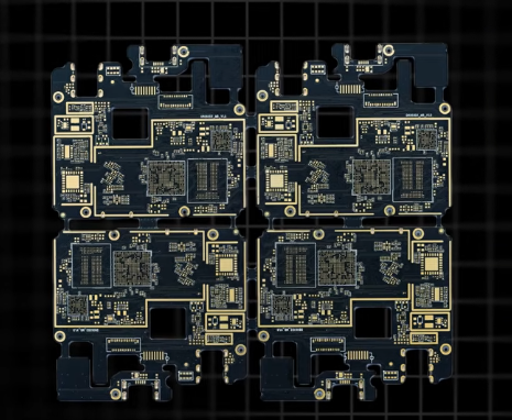
I. Technical Characteristics of Smartphone HDI Boards
HDI (High-Density Interconnect) is an advanced technology that enhances the routing capacity per unit area of a PCB through the use of micro-blind vias, buried vias, fine-line circuitry, and a multi-layer build-up structure.
Within a smartphone, HDI boards are primarily used for the mainboard, RF (radio frequency) circuit boards, camera module interconnect boards, power management modules, and various functional sub-boards.
Compared to traditional multi-layer PCBs, smartphone HDI boards offer the following characteristics:
Higher Routing Density
By utilizing fine-line circuitry with narrower trace widths and tighter spacing, these boards accommodate a greater number of signal connections within a limited area. This meets the high-density layout requirements for processors, memory, RF chips, and power management ICs.
Micro-via Interconnection Structure
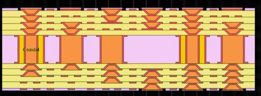
Micro-blind vias are created via laser drilling and subsequently filled using electroplating, enabling vertical connections between different circuit layers. Compared to traditional through-hole structures, this approach reduces the space required for routing and improves fan-out design for high-density components.
Multi-layer Build-up Design
Smartphone HDI boards can employ various build-up structures—such as 1+N+1 or 2+N+2 configurations—as well as more advanced “Any-Layer” (ELIC) interconnection technologies. The specific structure chosen depends on factors such as product dimensions, component pin density, and electrical performance requirements. 4. Thinness, Lightness, and High Integration
Integrating more functional circuits within the limited space of a motherboard, while ensuring adequate connectivity space for the processor, memory, communication modules, camera systems, and power supply units.
II. Structural Design of HDI (High-Density Interconnect) PCBs for Smartphones
The performance of an HDI PCB for a smartphone is largely determined during the design phase. Circuit architecture, interlayer connectivity, material selection, and impedance planning all directly influence the quality of subsequent PCB fabrication and PCBA (PCB assembly) processes.
Multilayer Circuitry and Build-up Structures
Modern smartphone motherboards must simultaneously handle digital signals, RF (radio frequency) signals, power signals, and high-speed data transmission; consequently, they typically employ a multilayer circuit structure.
In HDI structural design, signal, power, and ground layers must be strategically planned to minimize electromagnetic interference (EMI) between different signals.
For high-density processor packaging areas, “fan-out” routing—coordinated with the pitch of BGA (Ball Grid Array) pads—is essential to prevent circuit congestion that could compromise pad connections or manufacturability.
Micro-blind Via and Buried Via Design
Micro-blind vias are a critical component of smartphone HDI PCBs. They are generally formed via laser drilling, followed by copper electroplating to establish conductive connections.
In high-density regions, designers may choose between “stacked” or “staggered” via configurations, depending on available routing space.
Stacked vias increase vertical interconnect density but impose stricter requirements on via-barrel copper quality, via-filling performance, and thermal reliability. Staggered vias help distribute thermomechanical stress but require more routing space.
Therefore, engineering design must strike a balance between interconnect density, manufacturing costs, and long-term reliability.
High-Speed Signals and Impedance Control
Smartphone processors, memory modules, high-speed interfaces, and RF communication systems place high demands on PCB signal integrity.
HDI circuit design must focus on the following:
Controlled impedance and differential pair routing.
Signal return paths and the continuity of reference planes.
Crosstalk and electromagnetic interference (EMI) affecting high-frequency signals.
The length of critical signal traces and the number of vias used.
Power integrity and the control of power supply noise. For high-speed differential signals in particular, one should not focus solely on trace length; rather, simulation and verification must be conducted by accounting for material dielectric properties, the layer stack-up structure, and actual manufacturing parameters.
III. Manufacturing Process for Smartphone HDI (High-Density Interconnect) PCBs
The manufacturing precision of an HDI PCB directly impacts the quality of subsequent component assembly. For smartphone HDI PCBs, key control points include microvia formation, circuit patterning, interlayer registration, and copper electroplating.
High-Precision Circuit Fabrication
Circuits are formed through fine-feature pattern transfer and etching processes. For higher-density designs, advanced circuit fabrication techniques—such as the modified semi-additive process (mSAP)—may be employed.
The primary objective is to enhance circuit precision and minimize dimensional variations, ensuring sufficient routing space within high-density BGA (Ball Grid Array) regions.
Laser Drilling and Microvia Plating
Laser drilling is used to create micro-blind vias. Subsequent processes—including desmear, cleaning, electroless copper deposition, and electroplating—establish reliable conductive pathways between layers.
For smartphone HDI PCBs that require stacked vias, the process also involves copper via-filling and planarization.
Issues such as voids within filled vias, poor interface quality at the bottom of the via, or non-uniform copper thickness can pose potential reliability risks.
Sequential Lamination and Interlayer Registration
Multi-stage (any-layer or high-order) HDI structures typically require multiple sequential lamination cycles. Throughout the manufacturing process, it is critical to strictly control material expansion, lamination temperature, pressure, and the precision of interlayer registration.
Excessive interlayer misalignment can lead to misaligned microvias, inadequate pad connections, or abnormal spacing between circuits.
Surface Finish and Final Inspection
Smartphone HDI PCBs require a surface finish—such as ENIG (Electroless Nickel Immersion Gold) or OSP (Organic Solderability Preservative)—selected based on the specific requirements of the subsequent assembly process.
Furthermore, techniques such as AOI (Automated Optical Inspection), impedance testing, electrical continuity testing, and cross-sectional analysis are used to inspect for circuit defects, ensure the quality of copper within vias, and verify the integrity of interlayer connections.
IV. Key Assembly Processes for Smartphone HDI PCBs
Once the HDI PCB has been manufactured, it proceeds to the PCBA (Printed Circuit Board Assembly) stage. The key to assembling High-Density Interconnect (HDI) boards for smartphones lies in the precise placement of highly integrated chips and miniature electronic components onto intricate circuit boards, while ensuring the quality of solder joints and the stability of electrical connections.
Incoming Material Inspection and PCB Pre-treatment
Before assembly, HDI boards for smartphones must undergo inspections for appearance, dimensions, pad condition, surface finish, and warpage.
Key checks include:
Verifying that PCB pads are free from oxidation, contamination, and scratches.
Ensuring that micro-via filling and surface flatness meet specifications.
Checking for any anomalies on BGA pads and fine-pitch pads.
Confirming that the PCB’s flatness meets the requirements for component placement and reflow soldering.
For materials prone to moisture absorption, baking and moisture-control protocols—as specified by the material supplier—must be followed to prevent delamination or blistering during the reflow soldering process.
Solder Paste Printing
Solder paste printing is a critical stage in the assembly of smartphone HDI boards.
Given the presence of numerous fine-pitch components, miniature passive components, and BGA packages on the motherboard, the process demands high precision regarding stencil aperture design, solder paste particle size, squeegee pressure, and alignment accuracy.
Following the printing process, Solder Paste Inspection (SPI) equipment is typically used to measure the volume, height, area, and positional offset of the solder paste.
This step aims not only to minimize defects such as insufficient solder, excess solder, or solder bridging, but also to ensure a consistent supply of solder for the subsequent component attachment.
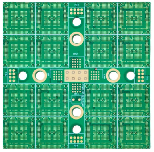
High-Precision SMT Placement
The assembly of smartphone HDI boards involves a wide variety of packaged components, including:
CPUs and application processors.
LPDDR memory and UFS storage.
Power Management ICs (PMICs).
RF front-end and communication chips.
Wi-Fi, Bluetooth, and related connectivity components.
Interfaces for cameras, power systems, and sensors.
SMT placement equipment must perform precise positioning based on component package specifications, pad locations, and the board’s fiducial markers. For fine-pitch BGA, LGA, and miniature passive components, it is critical to strictly control placement offset, placement pressure, and component coplanarity to prevent issues such as misalignment, “tombstoning,” cold/weak solder joints, and pad damage.
Reflow Soldering Temperature Control
Reflow soldering is a vital quality control stage in the assembly of high-density interconnect (HDI) PCBs for smartphones.
Given that smartphone motherboards feature multi-layer structures, a variety of package sizes, and high component density, the thermal capacity across different areas of the PCB is not uniform.
Consequently, the reflow soldering process requires a temperature profile tailored to the specific solder paste alloy, the thermal tolerance of the components, and the material properties of the PCB.
Particular attention must be paid to the preheating, soak (constant temperature), peak temperature, and cooling phases to avoid excessive localized temperature differentials, which could compromise the quality of the solder joints.
For smartphone HDI PCBs with double-sided component placement, it is also necessary to evaluate the impact of the second reflow pass on the solder joints of the components located on the underside.
BGA Soldering and Fine-Pitch Interconnections
Processors, memory modules, and certain communication chips typically utilize high-density packaging, with solder balls positioned beneath the chip—making it impossible to inspect the internal solder joints via standard optical methods.
Therefore, the assembly of smartphone HDI PCBs requires the use of X-ray inspection to analyze factors such as solder ball positioning, solder joint morphology, the presence of voids, and potential bridging.
For devices with high pin density, process validation must also account for package dimensions, pad design, and the reflow temperature profile.
V. Quality Control in Smartphone HDI PCB Assembly
Smartphone interiors are space-constrained, housing a large number of components with complex electrical interconnections. A defect in even a single solder joint can impair the device’s communication, charging, camera functionality, or overall system stability.
Thus, quality control cannot rely solely on visual inspection; instead, a comprehensive system must be established that encompasses PCB fabrication, SMT assembly, and functional verification.
Automated Optical Inspection (AOI)
AOI is primarily used to detect issues such as placement offsets, missing components, incorrect polarity, abnormal solder joint appearance, and visible solder bridges.
For high-density smartphone HDI PCBs, inspection criteria must be carefully defined based on component dimensions, pad configurations, and the specific capabilities of the inspection equipment.
X-Ray Inspection of Internal Solder Joints
X-Ray inspection is primarily used for examining hidden solder joints, such as those in BGA (Ball Grid Array) and LGA (Land Grid Array) packages. It helps identify defects including solder ball anomalies, bridging, and voids.
For the assembly of HDI (High-Density Interconnect) boards in smartphones, X-Ray inspection serves as a critical method for analyzing the quality of high-density packaging.
ICT and Electrical Testing
In-Circuit Testing (ICT) utilizes a layout of test points and specific test schemes to verify individual components and circuit connections, detecting issues such as open circuits, short circuits, and abnormal parameters in specific components.
Due to the limited space on HDI boards, it is not always feasible to place traditional probe test points across the entire board. Consequently, testing strategies must integrate boundary-scan techniques, in-circuit testing, and specialized test fixtures.
Full-Board Functional Testing
Following basic electrical testing, the smartphone HDI board must undergo functional verification.
Key areas include:
Communication between the main processor and memory.
Power management and charging functions.
RF (Radio Frequency) communication and antenna interfaces.
Camera operation and image data transmission.
Display, touch functionality, and peripheral interfaces.
Wireless connectivity, such as Wi-Fi and Bluetooth.
When necessary, the board may also undergo high/low-temperature operation tests, thermal cycling, mechanical vibration testing, and drop testing to evaluate its stability under real-world usage conditions.
VI. Key Technical Challenges in Smartphone HDI Board Assembly
Compared to PCBs used in standard consumer electronics, the assembly of smartphone HDI boards demands a higher level of engineering collaboration and process control.
First: Circuit density and manufacturing precision.
As circuit density increases, the management of tolerances—such as micro-via alignment, trace width/spacing, and pad dimensions—becomes increasingly critical, requiring early collaboration between PCB design and manufacturing processes.
Second: Reliability of micro-via structures.
While stacked micro-vias can enhance routing density, the thermo-mechanical stress between these vias requires careful evaluation. Particular attention must be paid to the quality of the copper plating within the vias, the integrity of via-filling, and the performance of dielectric materials, especially under conditions involving multiple reflow soldering cycles and long-term temperature fluctuations.
Third: PCB warpage and package coplanarity.
Thin HDI boards are highly susceptible to deformation caused by their material structure, copper distribution, and thermal stress. Warpage can lead to open circuits in BGA solder joints, component placement shifts, and uneven soldering.
Fourth, high-speed signals and electromagnetic compatibility (EMC).
Smartphones integrate a variety of wireless communication systems and high-speed digital circuits, requiring systematic control across areas such as stack-up design, grounding, impedance matching, and power integrity.
Fifth, balancing manufacturing costs and yields.
Higher-tier HDI (High-Density Interconnect) structures entail more complex sequential lamination, microvia fabrication, and inspection requirements. Engineering teams must carefully select technical approaches by weighing product performance, manufacturing capabilities, and target costs.
VII. Development Trends in Smartphone HDI PCB Assembly
Driven by the evolution of 5G communications, AI-enabled smartphones, multi-camera systems, and high-performance mobile computing, PCB designs within smartphones are trending toward higher integration and increasingly complex interconnect structures.
Moving forward, the assembly of smartphone HDI PCBs will place greater emphasis on the following areas:
Advanced HDI and Any-Layer Interconnects: Enhancing routing flexibility in BGA regions and shortening internal interconnect paths.
Advanced Circuit Fabrication Technologies: Utilizing processes such as mSAP (modified Semi-Additive Process) to meet the demands of ultra-high-density circuit designs.
High-Integration Packaging: Leveraging SiP (System-in-Package), PoP (Package-on-Package), and other advanced chip-packaging solutions to maximize functional integration within limited space.
Precision Automated Assembly: Employing high-accuracy placement equipment, along with SPI (Solder Paste Inspection), AOI (Automated Optical Inspection), and X-ray inspection, to ensure production consistency for complex PCBAs.
Reliability and Process Traceability: Strengthening end-to-end management of material batches, reflow soldering parameters, inspection data, and product test results.
VIII. Engineering Capabilities for Smartphone HDI PCB Assembly Services
For smartphone manufacturers and electronics R&D firms, selecting an HDI PCB assembly provider requires looking beyond mere SMT placement speeds or per-board processing costs; it necessitates a comprehensive evaluation of the provider’s overall engineering and manufacturing capabilities.
Key considerations include experience with high-tier HDI boards, proficiency in microvia structure fabrication, fine-pitch SMT placement, BGA soldering control, automated inspection, functional testing, and mass-production management. Furthermore, suppliers must possess capabilities in collaborative PCB design, DFM (Design for Manufacturability) assessment, BOM (Bill of Materials) management, process validation, and failure analysis.
From engineering development through to mass production, the assembly of HDI (High-Density Interconnect) boards for smartphones requires a comprehensive quality control process to ensure alignment across PCB architecture, component packaging, soldering processes, and overall device functionality.
Summary
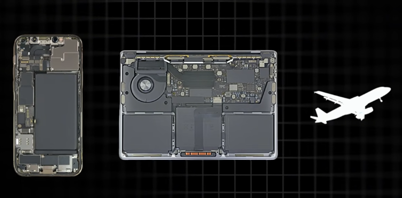
The assembly of HDI boards for smartphones goes beyond merely mounting electronic components onto a PCB; it is an integrated engineering discipline that encompasses high-density circuit design, micro-via interconnects, advanced PCB manufacturing, precision SMT (Surface Mount Technology) assembly, and system-level reliability verification.
As smartphones evolve toward greater AI integration, higher performance, and a thinner, lighter form factor, HDI boards will play an increasingly critical role in motherboard integration, communication performance, power management, and high-speed data transmission.
Ultimately, a truly mature capability for smartphone HDI PCB assembly hinges on the level of synergy achieved across design, materials, manufacturing, component mounting, inspection, and quality management.