
In an era characterized by the rapid evolution of Embodied AI, industrial 3D vision inspection, Autonomous Mobile Robots (AMRs), and consumer-grade 3D sensing devices, the depth camera has emerged as the essential “eye” for intelligent hardware.
Depth cameras typically integrate an RGB sensor, an infrared (IR) emitter (such as a VCSEL or laser engine), an IR receiver (IR CMOS), and either a dedicated Time-of-Flight (ToF) processing chip or a high-performance FPGA/ISP.
Because depth camera PCBAs incorporate high-frequency/high-speed digital circuitry, sensitive analog signal processing, high-current pulsed light drivers, and high-precision opto-electro-mechanical co-planar packaging, their R&D and delivery cycles present significant technical challenges.

In traditional PCBA manufacturing, issues such as optical misalignment, point-cloud drift caused by thermal deformation, and the degradation of high-frequency signal integrity often necessitate multiple design iterations (“re-spins”), leading to delays in product time-to-market.
This article explores the underlying technical logic and engineering implementation pathways required to achieve high yields, high reliability, and fast-turnaround delivery for depth camera PCBAs. We examine this through five key dimensions: system architecture design, high-frequency/high-thermal-conductivity PCB stack-up strategies, high-precision SMT assembly processes, opto-electronic joint calibration, and supply chain collaborative delivery.
I. System Architecture and Core Technical Challenges of Depth Camera PCBAs
Depending on the primary sensing technology employed, depth cameras are generally categorized into three types: Structured Light, Binocular Stereo Vision, and Time-of-Flight (ToF). Regardless of the specific approach, a depth camera PCBA functions as a highly integrated system—a fusion of optics, mechanics, electronics, and computational processing.
High-Frequency, High-Speed Signal Transmission and Signal Integrity (SI)
High-Speed Data Interfaces: IR and RGB image sensors typically utilize MIPI CSI-2/CSI-3 interfaces, with single-lane data rates reaching 1.5 Gbps to over 2.5 Gbps. Connections between the backend depth-computing chip and the host controller often employ USB 3.1 Gen2 (10 Gbps) or PCIe 3.0/4.0 interfaces.
Phase Consistency Requirements: In binocular and Time-of-Flight (ToF) systems, the synchronization accuracy between left and right CMOS sensors—or between modulated optical signals—must reach the nanosecond (ns) or even picosecond (ps) range. This necessitates extremely stringent trace length matching and skew control.
Mixed-Signal Power (High/Low Voltage) and Nanosecond-Pulse-Driven Interference (EMC/PI)
VCSEL Driver Characteristics: The transmitter side of ToF and structured-light systems requires the generation of ultra-high-frequency, narrow pulses—typically in the nanosecond range (e.g., 1 ns – 10 ns)—with peak currents reaching several amperes (A).
Power Supply Noise Suppression: High-current pulses generate intense di/dt transient effects. If the impedance of the Power Distribution Network (PDN) is inadequate, noise can couple—via conduction or radiation—into the sensitive IR/RGB image acquisition circuitry. This leads to increased image noise and a sharp decline in the Signal-to-Noise Ratio (SNR) of the point-cloud data.
High-Density Interconnect (HDI) and Thermal Stress Management
Space Constraints: Depth cameras are often limited by the physical space available in AMR (Autonomous Mobile Robot) heads or handheld devices. Consequently, PCBs typically utilize multi-layer, micro-via HDI structures (such as 1b/2b/3b or “Any-layer” HDI).
Coefficient of Thermal Expansion (CTE) Matching: VCSEL components and high-performance depth-processing (ISP) chips generate significant heat. Localized temperature increases can cause the PCB to undergo micron-scale thermal warping, which shifts the alignment of the optical lens axis and directly results in depth-measurement errors.
II. DFM/DFA/DFT Design Specifications for Rapid Delivery
To achieve a rapid response—from the freezing of the schematic for a depth-camera PCBA to the delivery of the first article (FATP)—it is essential to eliminate all potential manufacturing pitfalls during the New Product Introduction (NPI) design phase. This is accomplished by implementing “concurrent DFM (Design for Manufacturability) reviews,” ensuring that the design is inherently optimized for manufacturing.
Stack-up Optimization and PCB Material Selection
Material Selection Strategy:
High-speed digital sections: It is recommended to use “medium low-loss” or “very low-loss” grade FR-4 materials (such as Panasonic Megtron 4/6 or ShengYi S1000-2M), ensuring a dielectric constant (Dk) between 3.6 and 3.8, and a dissipation factor (Df) of less than 0.008.
Optical emission/thermal management sections: Utilize high-thermal-conductivity aluminum or copper-based substrates. Alternatively, incorporate embedded copper blocks or high-density thermal via arrays within the FR-4 stack-up, ensuring a thermal conductivity of at least 2.0 W/m·K.
Typical 8-layer HDI Symmetrical Stack-up Architecture (e.g., 1+N+1 configuration):
| Layer | Signal Type / Function Definition | Copper Thickness (OZ) | Dielectric Thickness / Process Notes |
| L1 (Top) | High-Speed Signal / Optical Components | 0.5 oz | ENEPIG surface finish, mixed micro-assembly and SMT |
| L2 (Inner) | Ground (GND) Plane | 0.5 oz | Solid reference ground plane, laser microvias (L1-L2) |
| L3 (Inner) | High-Speed Differential Line (MIPI/USB) | 0.5 oz | Strictly controlled impedance 90Ω / 100Ω |
| L4 (Inner) | Power Plane (Laser Driver VDD) | 1.0 oz | Dedicated split for high-current pulse power supply |
| L5 (Inner) | Power Plane (Digital Core VDD) | 1.0 oz | Core logic power plane alignment |
| L6 (Inner) | Signal / Control Lines | 0.5 oz | Low-speed control lines, GPIO, I2C |
| L7 (Inner) | Ground (GND) Plane | 0.5 oz | Solid shielding ground plane for sub-top layer |
| L8 (Bottom) | Bottom Signal / Thermal Pad Out | 0.5 oz | Auxiliary component placement and thermal via breakout |
Packaging and BGA Routing Rules
BGA/CSP Fan-out Strategy: High-performance computing chips typically utilize BGA packages with a pitch of 0.4mm–0.5mm. The design must consistently employ a “Via-in-Pad” process—incorporating resin-filled vias and a planarized, electroplated surface (POFP). The use of standard, externally routed vias is strictly prohibited to minimize high-frequency parasitic inductance.
Optical Sensor Pad Design: Pads for IR CMOS and VCSEL chips require extremely high positional accuracy (with symmetry controlled to within ±10 μm). The choice between Solder Mask Defined (SMD) and Non-Solder Mask Defined (NSMD) pads must be strictly determined based on the optical alignment geometric references provided by the sensor manufacturer.
Design for Testability (DFT) and Provisions for Automated Test Fixtures
Test Point Coverage: 100% coverage must be provided for test points on high-speed signal lines, power rails, and critical control signals (RESET, CLK, PWDN) on both the top and bottom layers. A minimum spacing of 0.8mm between test points is required to accommodate Flying Probe testing or In-Circuit Testing (ICT) during rapid-turnaround production.
ToF Modulation and VCSEL Calibration Interfaces: Dedicated low-parasitic-capacitance coaxial test connectors (Mini-RF connectors) or high-frequency probe points must be included to allow for the direct capture of nanosecond-scale VCSEL pulse waveforms at the PCBA stage.
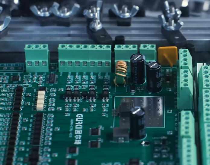
III. In-depth Hardware Design Analysis for High-Frequency/High-Speed and Nanosecond-Scale High-Current Driving
Engineering Techniques for High-Speed MIPI CSI-2/CSI-3 and USB 3.1 Routing
Impedance Matching and Differential Pair Control:
MIPI differential pairs must be controlled to 100Ω ± 8%, and USB 3.1 differential pairs to 90Ω ± 8%.
All traces must maintain a continuous reference to a solid ground plane; crossing over split power planes (split planes) is strictly prohibited. When transitioning between layers, at least one pair of GND stitching vias must be placed within 0.5 mm of the signal via to provide a continuous return path.
Length Matching and Skew Control:
The length mismatch between P/N signal traces within the same pair must be kept below 0.15 mm (phase difference < 2°).
The length mismatch between clock channels and data channels must be kept below 0.5 mm.
When using serpentine traces for length compensation, the radius of the bends should be ≥ 3 × trace width, and the spacing (S) between the serpentine segments should be ≥ 4 × trace width to prevent near-end crosstalk.
Power Integrity (PI) Design for High-Current, Narrow-Pulse VCSEL/Laser Driver Circuits
To ensure that a ToF depth camera can output sharp pulse waveforms at modulation frequencies in the tens of megahertz (MHz) range, the power distribution network (PDN) on the transmitter side must be optimized:
Reducing Loop Inductance:
The VCSEL, driver IC, and decoupling capacitors must be placed on the same side of the PCB, and the loop area formed by these components must be minimized (< 10 mm²).
Use wide copper pours instead of standard traces for power and ground routing, and employ multiple parallel vias to reduce via inductance.
Multi-Stage Decoupling Capacitor Configuration:
Place high-frequency ceramic capacitors (X7R/X5R, ESR < 10 mΩ) in 0201 or 01005 packages as close as possible to the driver IC pins.
Implement a tiered capacitor network—combining 0.1 µF, 1 µF, and 10 µF values—to cover the required impedance range from 10 MHz to 1 GHz, ensuring that the PDN impedance remains below the target impedance (Ztarget) across the operating frequency band.
IV. High-Precision SMT Manufacturing and Process Control for Depth Camera PCBAs
Depth camera PCBAs impose significantly higher requirements on the SMT (Surface Mount Technology) assembly process compared to conventional electronic products. The critical factors are placement accuracy and coplanarity, both of which directly determine the success rate of subsequent optomechanical calibration.
Solder Paste Printing and SPI (Solder Paste Inspection) Control
Precision Stencil Aperture Design:
For components with a 0.4mm pitch (such as BGAs) and ultra-small components (such as 0201s), use laser-cut, electro-polished “Fine Grain” (FG) stainless steel stencils or step-stencils.
For the thermal pads located beneath sensors and light-emitting chips (e.g., VCSELs), the stencil apertures should feature a “matrix window” (grid-pattern) design. The aperture ratio should be controlled between 60% and 70% to ensure that gases can escape during the reflow soldering process, thereby preventing an increase in voiding.
100% SPI Inspection Standards:
Solder paste volume must be maintained within 80%–120% of the target.
Offset must be controlled to ≤ ± 10 μm. Any instances of excessive voiding or insufficient solder are classified as defects and must be intercepted immediately.
High-Precision Component Placement and BGA/Sensor Alignment
Pick-and-Place Machine Precision:
The placement of image sensors (IR/RGB sensors) and VCSEL chips requires high-precision pick-and-place equipment (such as ASM Siplace or Fuji NXT systems) equipped with high-resolution vision systems. The placement accuracy must reach ± 10 μm at 3σ.
Fiducial Mark Design: Dedicated local fiducial marks should be placed diagonally relative to the optical sensor. This eliminates cumulative errors caused by potential board-level warpage or deformation.
Reflow Soldering: Temperature Profile and Warpage Control
Nitrogen (N2) Reflow: The entire process is conducted under a nitrogen atmosphere (with oxygen concentration maintained below 100 ppm) to enhance wettability, minimize pad oxidation, and ensure consistent melting of fine-pitch solder joints.
Warpage Control:
A 10-zone, double-sided heating reflow oven is utilized to regulate the temperature ramp rate (kept below 1.5 °C/sec), thereby reducing thermal shock.
For thin HDI boards (approximately 1.0 mm thick), high-precision SMT reflow carriers (jigs)—fabricated from synthetic stone or aluminum alloy—are employed. Equipped with clamps and positioning pins, these carriers strictly limit board warpage to less than 0.5%.
Cleaning and Underfill Processes
Aqueous Cleaning and Removal of Polar Contaminants: Prior to optical chip placement (or following protective packaging), high-pressure aqueous cleaning or ultrasonic cleaning is performed to ensure no flux residue remains around the solder pads, preventing light scattering and mold growth.
Underfill Dispensing: For large-format BGA components and stress-sensitive sensor chips, a “bottom underfill” process is applied, followed by thermal curing. This significantly enhances the PCBA’s resistance to mechanical stress and drop-related damage.
V. Integrated Optoelectronic Testing, Calibration, and Quality Assurance/Control (QA/QC)
Once the PCBA for a depth-sensing camera has completed the SMT assembly process, its electrical functionality is verified; however, to ensure the product is “ready for use upon delivery,” it must undergo rigorous integrated optoelectronic testing and collaborative software-hardware calibration.
Electrical Performance Testing (AOI + AXOI / ICT)
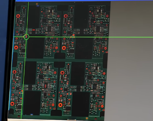
3D AOI (Automated Optical Inspection): Used to detect missing, misplaced, or reversed components, as well as defects such as “tombstoning,” cold/poor solder joints, and irregularities in the geometry of surface-mounted solder fillets.
3D AXI (X-Ray Inspection): Performs 100% penetration scanning of BGA and QFN bottom pads, as well as internal bonding wires within sensors. This ensures a voiding rate of < 10% for solder pads, with no bridging or solder beads.
Hardware-Level Electro-Optical (E-O) Testing
PCBA power-on testing conducted within a shielded, dark environment:
VCSEL Optical Power and Wavelength Testing: Utilizes an integrating sphere and spectrometer to measure the peak power and wavelength (e.g., 850nm / 940nm) drift of the infrared emitter under various pulse-driven conditions.
Sensor Dark Current and Noise Testing: Captures raw image data from IR/RGB CMOS sensors in the absence of light to calculate Fixed Pattern Noise (FPN) and Temporal Noise.
Depth Calibration and Point Cloud Quality Verification
For rapid delivery solutions, services such as “PCBA + lens pre-assembly” or “module pre-calibration” are available:
Intrinsic Calibration: Employs high-precision checkerboard or dot-array calibration targets to automatically calculate focal lengths (fx, fy), principal points (Cx, Cy), and distortion coefficients (k1, k2, p1, p2).
Extrinsic Calibration (for binocular or structured-light systems): Determines the rotation matrix (R) and translation vector (T).
Point Cloud Accuracy Assessment: Evaluates Z-axis absolute accuracy, relative accuracy (precision/noise standard deviation), and fill rate at typical distances of 0.5m, 1m, and 3m.
VI. Engineering Management and Supply Chain Coordination Strategy for “Rapid Delivery” of Depth Camera PCBAs
For R&D-driven enterprises or high-tech OEM/ODM firms, “speed” is the key to seizing market opportunities. Achieving a turnaround time as fast as 72 hours—from Gerber files to a finished PCBA—relies not merely on manufacturing speed, but on a fully automated, agile supply chain management system.
Agile Component Supply Chain and Standardized BOM Management
Strategic Safety Stock for Core Chips: We maintain strategic reserves—in collaboration with distributors—for components with long lead times, such as specialized ISPs (e.g., Intel RealSense chips, Orbbec-proprietary ASICs, FPGAs), VCSEL drivers, and other high-end integrated circuits.
Pre-vetted Cross-References: During the R&D DFM (Design for Manufacturing) phase, we identify 2–3 pin-to-pin compatible alternatives for passive components (resistors, capacitors, inductors), LDOs, and MOSFETs—sourcing from reputable brands like Murata, TDK, TI, ADI, and Nexperia—to ensure that a shortage of a single component does not halt the entire production line.
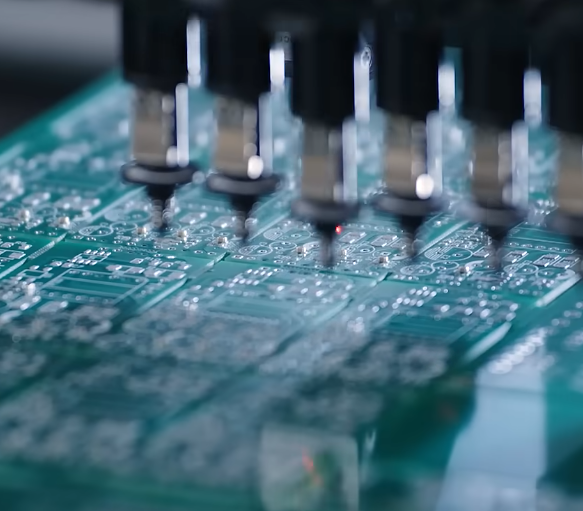
Modular NPI (New Product Introduction) Engineering Response Mechanism
Rapid CAM Pre-screening: Utilizing fully automated software (CAM 350 / Genesis) to parse Gerber files, we generate Engineering Queries (EQs) within two hours, supported by an online, closed-loop collaboration process with R&D engineers.
Parallel Development of Stencils and Fixtures: Once CAM data is verified, we immediately initiate the production of SMT stencils, offline SMT programming, and the development of ICT (In-Circuit Test) fixtures—all in parallel—to minimize lead times.
Control Matrix for Rapid-Delivery Engineering Management
| Stage | Core Tasks | Fast-Turn Time | Standard Time |
| Stage 1: DFM & Procurement | Gerber/BOM review, material kitting, CAM engineering generation | 2 – 4 Hours | 24 – 48 Hours |
| Stage 2: Bare PCB Fabrication | 8-layer HDI quick-turn prototype (including laser drilling & POFP via-in-pad filling) | 24 – 48 Hours | 5 – 7 Days |
| Stage 3: SMT Assembly | Stencil fabrication, SMT placement, reflow soldering, 3D AOI/AXI inspection | 12 – 24 Hours | 2 – 3 Days |
| Stage 4: Testing & Calibration | ICT testing, optoelectronic functional testing, point cloud calibration | 6 – 12 Hours | 1 – 2 Days |
| End-to-End Turnaround | From file sign-off to finished PCBA ex-factory dispatch | As fast as 48 – 72 Hours | 10 – 14 Days |
Summary
The rapid delivery of PCBA solutions for depth cameras is a complex systems engineering endeavor that integrates high-frequency/high-speed design, EMC control, thermal stress management, micro-assembly, and optoelectronic calibration.
As an industry-leading, one-stop PCBA service provider specializing in professional PCB assembly and manufacturing, KingTop Technology implements DFM (Design for Manufacturing) and DFA (Design for Assembly) standards from the very beginning of the design phase.
Through meticulous control of component placement and reflow soldering—supported by our proprietary, highly efficient optoelectronic calibration production lines and an agile supply chain—we overcome the traditional industry bottlenecks of high technical barriers and long lead times. This enables us to deliver high-quality products with high yields at exceptional speed, fully empowering the rapid commercial deployment of embodied AI and industrial vision systems.