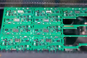
Service robots are rapidly transitioning from laboratories and controlled demonstration zones into complex, dynamic environments—ranging from commercial delivery and medical assistance to smart agriculture, high-altitude operations, and home companionship.
Unlike general consumer electronics (such as smartphones or tablets) or traditional industrial robotic arms, service robots are characterized by high mobility, adaptability to changing environments, extensive multi-sensor fusion, and stringent safety standards for human-robot interaction.
These characteristics present unique and highly demanding engineering challenges for Service Robot PCB Assembly (SR-PCBA).
At the hardware manufacturing level, an SR-PCBA is far more than a simple carrier for soldering electronic components; it functions as a “miniature electromechanical nerve center” that integrates high-performance edge computing, high-dynamic-range motor driving, signal conditioning for heterogeneous multi-source sensors, and intelligent power management.
I. System Architecture and Modular Decoupling of Service Robot PCBAs
The electronic systems of service robots typically adhere to design principles of “hierarchical partitioning, heterogeneous parallel processing, and modular decoupling.” In actual assembly and manufacturing, different functional modules impose significantly different requirements regarding PCB materials, layer stacking, copper thickness, and component packaging.
Main Computing & Perception Hub PCBA (AI Computing & SLAM Navigation)
Architectural Features: Equipped with high-performance SoCs (such as the NVIDIA Jetson AGX/Orin series, Rockchip RK3588, or x86-based embedded CPUs) to run the Robot Operating System (ROS), real-time SLAM mapping, 3D object detection, and path planning.
Process and Material Requirements:
High-Density Interconnect (HDI): Typically utilizes an 8- to 14-layer board structure, incorporating first- or second-order blind/buried vias or even Any-Layer HDI technology.
Fine Pin Pitch: BGA packages typically feature ball pitches as small as 0.4mm–0.5mm, placing extremely high demands on pad design (NSMD vs. SMD) and SMT placement accuracy.
Material Selection: Uses medium/high Tg FR-4 or Low-Dk/Low-Df high-frequency, high-speed materials (such as Panasonic Megtron 4/6) to ensure signal integrity for high-frequency differential signals like PCIe 4.0/5.0, USB 3.2, and MIPI CSI.
High-Dynamic-Range Motor Drive and Motion Control PCBA (Motion & Servo Drive PCBA)
Architectural Features: Service robots (especially legged robots, wheeled-tracked hybrid robots, and multi-axis robotic arms) require frequent start/stop, emergency stop, reversal, and torque response operations; drive boards must withstand high peak currents and back-electromotive force (Back-EMF).
Manufacturing and Material Requirements:
Heavy Copper PCB Technology: Copper trace thicknesses of 2oz, 3oz, or even 4oz are commonly used to minimize resistive heating effects when conducting high currents.
Power and Signal Isolation: Strict separation between the high-voltage/high-current drive section (e.g., MOSFET/IGBT bridge legs) and the low-voltage MCU/DSP control logic section is achieved via optocouplers or digital isolators (magnetic isolation).
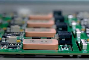
Heatsink and Thermal Path Design: Dense thermal via arrays are designed beneath power MOSFETs, complemented by embedded aluminum or copper base structures or rear-mounted metal heat spreaders.
Multi-Source Heterogeneous Sensor Fusion Interface PCBA (Sensor Fusion Interface PCBA)
Architectural Features: Connects components such as LiDAR, depth cameras (RGB-D), ultrasonic arrays, anti-drop infrared sensors, tactile sensors, and IMUs (Inertial Measurement Units).
Manufacturing and PCB Material Requirements:
Ultra-low noise power rails: The analog signal conditioning area requires high-PSRR (Power Supply Rejection Ratio) LDOs to prevent motor noise from coupling into sensitive sensor lines.
IMU mechanical and thermal stress isolation: IMU chips are extremely sensitive to minute PCB deformations and temperature gradients; assembly often involves cutting stress relief slots around the IMU chip or employing a spring-suspended design on a separate small daughterboard.
Smart Battery Management and Power Distribution PCBA (BMS & Power Distribution PCBA)
Architectural features: Responsible for the balanced charging and discharge protection of the lithium battery pack, as well as estimating State of Health (SOH) and State of Charge (SOC); also provides regulated voltage conversion (48V/24V/12V/5V) for the entire vehicle.
Manufacturing and PCB Material Requirements:
High-voltage safety spacing: Strict adherence to creepage and clearance standards.
High-voltage/high-current component soldering: Utilizes large-format SMD inductors and high-power shunt resistors; places extremely high demands on the mechanical strength and fill quality of solder joints.
II. Detailed Explanation of Key Manufacturing and SMT/THT Assembly Processes
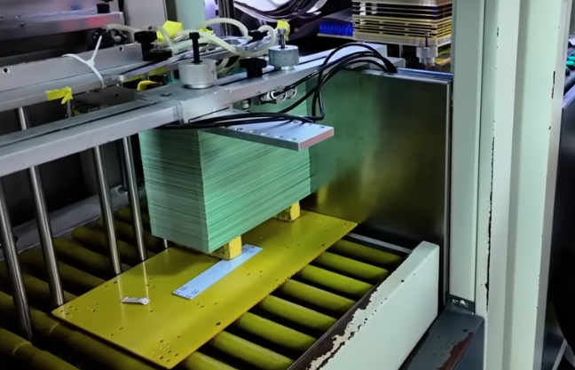
The assembly process for service robot PCBAs is far more than a simple “solder paste printing – component placement – reflow” sequence; it is a highly refined, fully traceable manufacturing engineering process.
Solder Paste Printing & 3D SPI Monitoring (Solder Paste Printing & SPI)
Nano-coated stencil technology: For boards featuring a mix of 0201/01005 passive components and 0.4mm pitch BGAs, laser-cut stencils with nano-coatings are used to optimize the solder paste release angle and transfer efficiency, significantly reducing the probability of solder bridging and insufficient printing.
Step-up/Step-down Stencil: Used when a single PCBA contains both fine-pitch ICs and high-current power components; the stencil thickness is locally increased or decreased to adjust the volume of solder paste deposition.
3D SPI (Solder Paste Inspection) – 100% Inspection: Performs 3D measurements of solder paste volume, area, height, and center offset after printing to prevent defects such as cold joints (caused by insufficient paste) or short circuits (caused by excessive paste).
High-Precision SMT Placement
Dual-lane, multi-head placement machine configuration:
High-speed placement head: Handles high-speed pick-and-place operations for 0201 and 0402 passive components (resistors/capacitors) and small SOT/SOP packages.
High-precision odd-form placement head: Equipped with a high-resolution vision system; specifically designed for large multi-pin components (BGA/QFN larger than 40mm x 40mm), large inductors, and shielding can terminals.
Placement pressure control: Allows for micron-level adjustment of nozzle placement pressure—critical for thin BGAs or flexible PCBs (FPC)—to prevent damage to component housings or solder paste bridging caused by excessive compression.
Nitrogen (N2) Reflow Soldering
Multi-zone temperature profile design: Utilizes reflow ovens with 10–12 independently controlled temperature zones.
Ramp-up Zone: Controls the heating rate (1.5°C/s–2.5°C/s) to prevent thermal shock damage to sensitive capacitors.
Soaking Zone: Allows components with high thermal mass (e.g., large inductors, heat sinks) and those with low thermal mass (e.g., small resistors/capacitors) to reach thermal equilibrium, ensuring full activation of the flux.
Reflow Peak Zone: Control the Time Above Liquidus (TAL) to 60–90 seconds and maintain the peak temperature between 235°C and 245°C (for the SAC305 lead-free process).
Nitrogen (N2) Atmosphere Control: Reduce the oxygen concentration inside the oven to below 500–1000 ppm to significantly minimize secondary oxidation on pads and component leads, enhance solder joint wettability, and strictly control the BGA solder joint void area to below 10%.
Hidden Solder Joints and 3D AOI/X-Ray Inspection
3D AOI (Automated Optical Inspection): Utilize multi-angle ring lighting and 3D projected grids to comprehensively inspect chip components for defects such as tombstoning, standing on edge, cold/poor solder joints, reversed polarity, and bridging.
3D AXI (Automated X-ray Inspection): For BGA, QFN, and BTC packages as well as exposed thermal pads, employ X-ray laminography (layer-by-layer scanning) to precisely calculate voiding percentages and detect internal bridging and solder bridging/whiskering.
Odd-form Through-hole Components and Selective Wave Soldering
Service robot circuit boards often feature numerous heavy-duty mechanical connectors (such as aviation-grade power sockets, motor phase terminals, and large-capacity aluminum electrolytic capacitors).
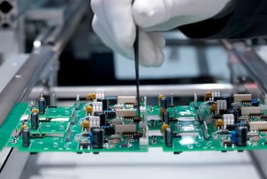
Manual Soldering vs. Selective Wave Soldering: Manual soldering quality is highly dependent on operator technique and lacks consistency; selective wave soldering utilizes CNC-controlled flux spraying and localized mini-wave dip soldering to achieve high-quality through-hole fill (targeting >75% fill) without damaging surrounding SMT components.
III. Innovative Technologies and Cutting-Edge Manufacturing Trends
As service robots evolve toward greater miniaturization, lighter weight, and higher reliability, traditional PCBA processes are witnessing the emergence of several breakthrough technologies.
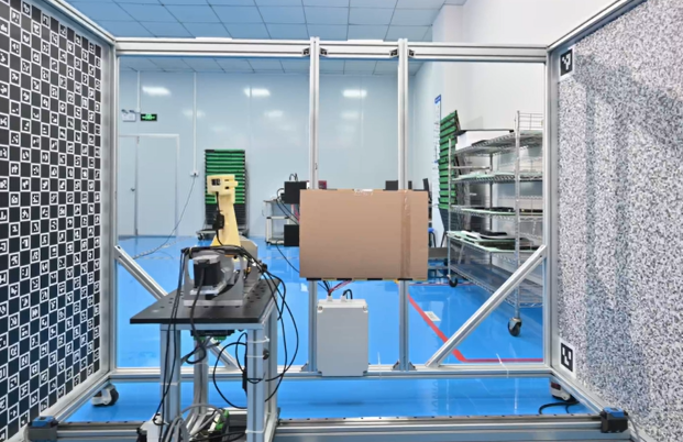
Rigid-Flex PCBs and 3D Assembly
Traditional service robots feature complex internal wiring; the extensive use of wire harnesses and connectors not only consumes space but also makes connections highly susceptible to loosening or failure due to frequent movement and vibration.
Rigid-Flex Design: Rigid boards (FR-4) and flexible boards (PI – polyimide) are laminated together during the PCB manufacturing stage to create a 3D, foldable circuit system.
Engineering Advantages:
Eliminates over 60% of board-to-board connectors and wire harnesses.
Significantly reduces the overall weight and volume of the unit, thereby increasing the robot’s payload capacity in confined spaces.
Substantially improves fatigue life regarding vibration resistance and tolerance to repeated bending.
Embedded Component Technology
To accommodate computing and drive modules within extremely compact spaces, some high-end service robots are adopting embedded PCB technology:
Passive Component Embedding: Surface-mount resistors and capacitors are embedded within the PCB’s inner dielectric layers, freeing up surface mounting area.
Chip Embedding (Embedded Die): Power MOSFETs or microcontroller chips are embedded directly within the PCB layers, utilizing copper bumps for electrical connections. This method eliminates the parasitic inductance associated with bond wires, reducing high-frequency switching losses by over 30% while significantly improving thermal conduction paths.
Underfill and Localized Reinforcement (Staking & Edge Bonding)
Service robots are subjected to transient impact forces of up to 20G–50G during drops, collisions, or obstacle traversal.
BGA Underfill: Utilizing capillary action, epoxy resin is injected beneath the BGA chip after reflow soldering; upon curing, it tightly encapsulates the BGA solder balls and the PCB. This process enhances the solder joints’ resistance to thermal cycling stress and mechanical shock by a factor of 5 to 10.
Corner/Edge Bonding for Heavy Components: Structural adhesives (single- or two-component) are applied to secure tall electrolytic capacitors, transformers, large inductors, and connector pins—either at three points or along all four sides—to prevent pad cratering caused by vibration.
In-situ Thermal Management and Metal Substrate Integration
For high-power joint motor drive boards (e.g., leg joint actuators in quadruped robots):
Copper Coin Insertion: A pure copper block is press-fitted directly beneath the MOSFET to conduct heat from the chip base to a large-area metal heat sink on the reverse side.
Insulated Metal Substrate (IMS / Aluminum PCB): An aluminum plate is laminated with a highly thermally conductive dielectric layer (thermal conductivity of 2.0–8.0 W/mK) and copper foil; SMD power transistors are mounted directly onto this structure to achieve ultra-low thermal impedance.
Automated Selective Conformal Coating and Nano-hydrophobic Coatings
Service robots are frequently exposed to complex or even harsh physical environments (e.g., moisture for cleaning robots, dust and salt spray for agricultural robots, and rain or snow for delivery robots).
Selective Conformal Coating: CNC coating machines are used to precisely spray acrylic, polyurethane, or silicone materials onto the PCB surface, automatically avoiding areas such as optical sensors, connector contacts, microswitches, and thermal interfaces.
Nano-hydrophobic Coating (Parylene / Nano-Coating): A nanoscale, ultra-thin, and non-porous protective film is formed on the PCBA surface via vacuum chemical vapor deposition (CVD). This achieves IPX6/IPX7-level water and dust resistance without interfering with high-frequency signal transmission or component heat dissipation.
IV. Challenges in the Reliability-Focused Design and Manufacturing of Service Robot PCBAs
A fundamental conflict exists between the industrial-grade service life requirements for service robots (typically necessitating continuous operation for over 3–5 years) and their complex, dynamic operating environments. Outlined below are the technical challenges that must be overcome during manufacturing, along with corresponding strategies:
| Challenge Dimension | Root Cause Analysis | Manufacturing & Assembly Countermeasures |
| Mechanical Vibration and Fatigue Peeling | Wheeled/tracked obstacle clearance and foot-step impact in legged robots induce high-frequency, low-amplitude bending and peeling stress on the PCB. | 1. Adopt high peel strength laminate materials; 2. Add Via-in-Pad with electroplating reinforcement; 3. Perform 100% Underfill dispensing on BGAs; 4. Optimize the distribution of mounting screw holes to avoid stress concentration areas. |
| Thermal Cycling and CTE Mismatch | Frequent startup heating and shutdown cooling of power drive modules trigger differential stress due to the Coefficient of Thermal Expansion (CTE) mismatch between the silicon chip and PCB (FR-4). | 1. Select high-grade Tg170+ laminate materials with low CTE values; 2. Use flexible, high-toughness lead-free alloy solders (e.g., SAC-Ni doped alloys); 3. Limit the number of reflow cycles (controlled within 2 times). |
| Electromagnetic Interference (EMI) and Crosstalk | High-frequency switching noise (several kHz to tens of kHz) from motor PWM drives couples into high-precision IMUs, encoders, and ultrasonic circuits. | 1. Strictly prohibit trace routing across split ground planes; 2. Adopt SMT frame with snap-on cover design for shielding cans; 3. Add copper pour shielding on sensitive traces and densely place ground stitching vias. |
| Conductive Anodic Filament (CAF) Growth | In high-humidity environments, copper ion migration easily occurs between dense biased vias, leading to internal micro-short circuits in the laminate. | 1. Specify anti-CAF grade FR-4 glass fiber laminate materials; 2. Maintain a spacing greater than 0.3mm between via to via, and via to trace; 3. Strictly control the baking process to eliminate moisture absorbed inside the board. |
V. Quality Control, Testing/Verification, and Full Lifecycle Traceability System
To ensure that every service robot PCBA leaving the factory meets industrial-grade “Zero Defect” standards, the manufacturing process must incorporate end-to-end automated testing and traceability management (MES).
Process Defect Control and Inspection
Strict IQC (Incoming Quality Control): Moisture-sensitive devices (MSD, such as BGA and QFN components) are handled in strict accordance with the J-STD-033 standard regarding unpacking, baking, and storage in moisture-proof cabinets; periodic sampling inspections are conducted on PCB pad solderability.
Ionic Contamination Test: Following assembly and cleaning (if a cleaning process is used), the residual ion content per square centimeter is measured to ensure levels remain well below IPC-6012 standard limits, thereby preventing subsequent electrical leakage and electrochemical corrosion.
Automated Board-Level Testing System (ICT & FCT)
ICT (In-Circuit Test / Bed-of-Nails Test): Detects open circuits, short circuits, resistance, capacitance, and inductance values across all PCB network nodes, as well as diode/transistor PN junction characteristics, enabling rapid identification of SMT soldering defects.
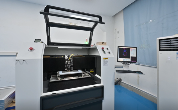
FCT (Functional Circuit Test):
Automated Test Fixtures: Utilizes pneumatic bed-of-nails fixtures and modular instruments (DAQ cards, oscilloscopes, electronic loads, CAN/RS485 analyzers) to simulate the electrical environment of the actual robot.
Automated Firmware Programming: Automatically programs the Bootloader and low-level driver firmware into the MCU/DSP via SWD, JTAG, or serial interfaces during the FCT stage.
Dynamic Load Response Testing: Applies dynamic electronic loads to motor drive channels to test over-current protection (OCP), over-voltage protection (OVP), and the sampling accuracy of the FOC (Field-Oriented Control) current loop. 3. Environmental Stress Screening (ESS)
High-Temperature Burn-in Test: PCBA units that have passed FCT are placed in a high-temperature burn-in chamber (60°C–85°C) and operated continuously under simulated loads for 24 to 72 hours to accelerate the identification and elimination of components prone to “infant mortality” (early-stage failure).
Combined Temperature/Humidity Cycling and Vibration Test (HALT/HASS): Highly Accelerated Life Testing (HALT) is performed on PCBAs during the R&D phase and via batch sampling during mass production. The units are subjected to rapid temperature cycling (-40°C to +125°C) and multi-axis random vibration to expose potential structural design flaws and risks associated with solder joint fatigue.
MES (Manufacturing Execution System) and Traceability
Each service robot PCBA features a laser-engraved DataMatrix code, enabling the MES to provide:
Component-Level Traceability: Precise recording of lot numbers, suppliers, and warehousing dates for resistors, capacitors, and IC chips used on the board.
Process Parameter Traceability: Linking the board to specific process data, including solder paste SPI images from the printing stage, SMT placement machine IDs, real-time reflow temperature profiles, X-ray inspection images, and FCT test data logs.
After-Sales Traceability: In the event of a robot malfunction, scanning the PCBA’s QR code allows for the rapid retrieval of the complete manufacturing history—even from years prior—providing a direct basis for quality improvement.
VI. Conclusion
Service robot PCB assembly has evolved beyond traditional Electronics Manufacturing Services (EMS) into a cutting-edge, interdisciplinary field that integrates materials science, thermodynamics, electromagnetics, precision mechanical engineering, and automated control. Driven by the rapid advancement of humanoid robots, Embodied AI, and industrial collaborative robots, the future of SR-PCBA manufacturing will be defined by four key trends:
Higher levels of integration: Technologies such as wafer-level packaging (WLP), 3D chip stacking, and 3D MID (Mechatronic Integrated Devices) will further reduce the size of controllers.
Enhanced intelligent manufacturing: AI-based visual prediction of solder joint defects and adaptive, dynamic adjustment of reflow soldering temperature profiles will push the First Pass Yield (FPY) of production lines to near-100% levels.
Greener, eco-friendly processes: Widespread adoption of low-temperature soldering (LTS) materials alongside no-clean and ultra-low VOC coating technologies.
Deeper hardware-software co-testing: Board-level testing will move beyond simple hardware connectivity checks to incorporate lightweight AI diagnostic models, ensuring optimal alignment between hardware and algorithmic baselines before the PCBA leaves the factory.
Precise process design, rigorous manufacturing control, and comprehensive reliability validation form the cornerstone of stable, safe, and efficient operation for service robots.
About KingTop Technology
As an industry-leading provider of microelectronics manufacturing and assembly services, KingTop Technology specializes in delivering high-quality, one-stop PCB assembly solutions for service robots to global clients. Leveraging deep technical expertise in multi-layer high-density HDI board manufacturing, thermal management designs for thick-copper motor drives, and high-precision mixed SMT/THT assembly, KingTop Technology precisely meets the rigorous technical requirements for mobile robots, AI computing control units, and sensor fusion boards. The company strictly adheres to high-standard quality systems such as IATF 16949 and ISO 13485, utilizing advanced equipment—including 3D SPI, 3D AOI, X-ray inspection, and selective conformal coating systems—to ensure the long-term stability and high reliability of robotic PCBA products amidst complex vibration, thermal cycling, and harsh operating environments.