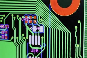
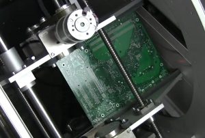
Driven by rapid advancements in cutting-edge fields such as industrial automation, humanoid robotics, medical surgical robots, and autonomous driving systems, the manufacturing process for the control core—the high-precision robot motherboard—faces unprecedented and rigorous challenges.
Unlike standard consumer electronics or general-purpose server motherboards, robot motherboards must not only support high-performance AI chips, DSPs, and FPGAs but also integrate multi-axis servo drive controls, high-precision sensor signal chains, high-current power management, and various industrial bus communication modules within extremely compact spaces.
The assembly process for high-precision robot motherboards (PCBA) encompasses a comprehensive engineering workflow, ranging from Design for Manufacturability (DFM) analysis and substrate selection to SMT (Surface Mount Technology) placement, 3D inspection, precision soldering, and final packaging and reliability verification for complex operating environments.
I. Core Technical Characteristics and Design Challenges
Ultra-High-Density Interconnect (HDI) and Complex Layer Architecture
High-precision robot motherboards typically utilize high-layer-count (12 to over 30 layers) HDI circuit board structures, widely employing technologies such as blind vias, buried vias, and Any-Layer HDI.
As chip pin pitches shrink to 0.3mm or less (e.g., in BGA and CSP packages), PCB designs must adopt “Via-in-Pad” technology combined with Via-in-Pad Plated Over (VIPPO) processes to prevent solder paste leakage and void formation during soldering.
Integrated Layout of Mixed Signals and High/Low-Voltage Power Systems
The robot motherboard requires the physical coexistence of “supercomputing power, high-sensitivity sensing, and high-power driving capabilities” within an extremely compact footprint:
Low-voltage and digital signal zone: Includes high-frequency CPUs, Neural Processing Units (NPUs), high-speed DDR5/LPDDR5 memory chips, and PCIe 5.0/6.0 buses; this area demands extreme precision regarding signal integrity (SI) and impedance control (e.g., maintaining a deviation within ±5%).
Analog and sensor interface zone: Includes gyroscopes (IMUs), encoder feedback, and microvolt-level torque sensor interfaces; this area is highly susceptible to electromagnetic interference (EMI).
High-voltage and power drive zone: Integrates MOSFET bridge drivers, high-current busbars, and DC-DC converters; it must withstand pulse currents ranging from tens to over a hundred amperes in short bursts while generating significant heat and electromagnetic noise.
Physical Design for High Vibration Resistance and Heat Dissipation under Extreme Conditions
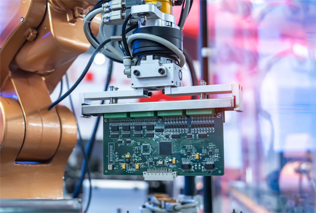
Robot operation involves continuous high-frequency vibration, mechanical shock, and drastic temperature fluctuations.
Motherboard assembly must account for:
Dynamic stress distribution: Preventing micro-cracking or fracture of BGA solder joints during high-speed robotic arm movements or collisions.
Thermal management architecture: Incorporating embedded copper or aluminum metal cores, thick copper layers (locally thickened to 2oz–4oz), and thermal via arrays to ensure unobstructed heat conduction paths for high-power components.
II. SMT Surface Mount Technology and High-Precision Process Flow
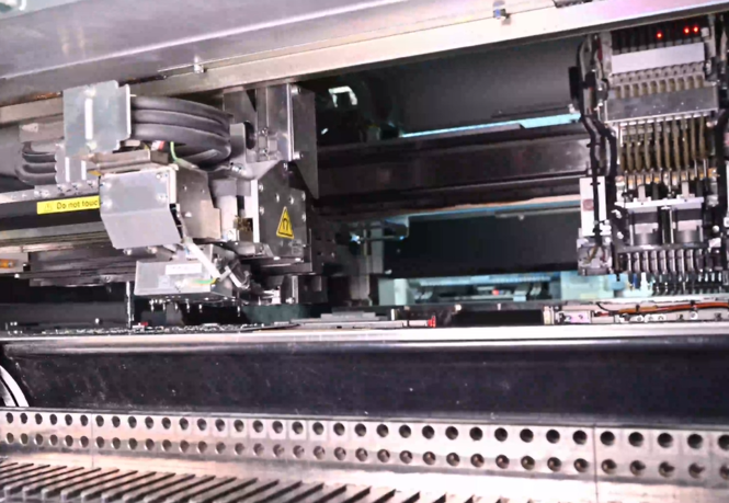
To ensure defect-free assembly of both ultra-fine-pitch components (such as 01005/03015 SMDs, BGAs, and QFNs) and heavy, large-scale components on the same board, the assembly process for high-precision robot motherboards requires rigorous control of fully automated SMT production lines.
High-Precision Solder Paste Printing and 3D SPI
Solder paste printing is critical to PCBA quality control; statistics show that over 60% of soldering defects originate in the printing stage.
Stencil Design: Nano-coated laser-cut stainless steel stencils or electroformed stencils are utilized. Step-up/step-down aperture designs are employed for 0.3mm pitch BGAs and 01005 components to precisely control solder paste release volumes across different zones.
3D SPI (Solder Paste Inspection): Laser 3D scanning technology is used to perform 100% inspection of solder paste volume, area, height, and offset. Strict alarm thresholds are set to prevent defects such as insufficient paste, excessive paste, bridging, and tombstoning.
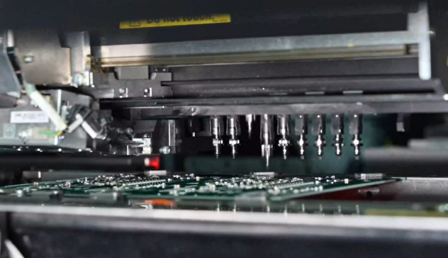
High-Speed and Odd-Form Component Placement (Pick and Place)
High-precision robotic mainboards contain a mix of ultra-miniature passive components (resistors, capacitors, inductors) and odd-form connectors, heavy heat sinks, and large BGAs.
Machine Vision and Fiducial Mark Recognition: Placement machines are equipped with high-resolution CCD cameras. They utilize global fiducial marks and local micro-fiducials for precise optical alignment of fine-pitch BGAs, achieving placement accuracy of ±15μm @ 3σ.
Dynamic Pressure Control: Real-time feedback control of placement pressure prevents bridging caused by solder paste squeeze-out (due to excessive pressure) or component drift (due to insufficient pressure).
Multi-Zone Nitrogen-Purged Reflow Soldering
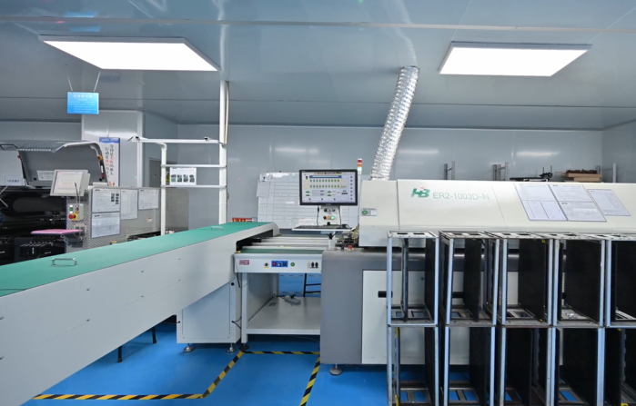
Reflow soldering is the critical step for achieving metallurgical bonding. High-precision robotic mainboards typically undergo reflow soldering in 10-zone or 12-zone ovens with a full nitrogen (N2) atmosphere.
Nitrogen Environment Management: By maintaining oxygen concentration between 100 ppm and 500 ppm, oxidation of molten solder and pads is drastically reduced, wettability is improved, and the void rate within BGA joints is significantly lowered.
Precision Real-Time Thermal Profiling: For assemblies featuring mixed board thicknesses and high-thermal-mass components, parameters are precisely set for the preheat zone, soak zone, reflow peak zone (typically 235°C–245°C for lead-free SAC305 systems), and cooling rate (controlled at 2°C–4°C/sec) to minimize thermal stress and prevent interlayer damage to the multilayer PCB structure.
III. Inspection Technologies and Non-Destructive Analysis for Quality Assurance
The high reliability required for robotics motherboards demands “zero-defect” delivery; the failure of any hidden solder joint could cause the entire system to malfunction. Consequently, the assembly process relies on multi-layered automated inspection methods.
3D AOI (Automated Optical Inspection)
Unlike traditional 2D AOI, which relies on planar comparison to identify defects, 3D AOI utilizes phase-shifting technology with multiple projection angles to capture the true 3D profiles of components and solder joints.
Inspection items: Tombstoning, billboarding, missing components, reversed polarity, wrong components, cold/weak joints, lead coplanarity issues, and solder fillet height.
3D AXOI / X-Ray Non-Destructive Inspection
X-ray inspection is essential for examining hidden solder joints located beneath BGA, CSP, and QFN packages.
Voiding Ratio Calculation: Utilizing 3D Computed Tomography (CT) technology, the system precisely calculates the percentage of void area relative to the total cross-sectional area of each BGA solder ball, strictly limiting the voiding ratio in critical joints to below 10% or 15%.
Bridging and Solder Bead Screening: X-rays penetrate high-density board layers to directly detect internal short circuits caused by solder wicking into via-in-pad structures. 3. First Article Inspection (FAI) and Flying Probe Test/ICT
When the first unit of a batch (First Article) is produced, an automated First Article Inspection system—combined with high-precision LCR measurement—is used to perform 100% verification of the electrical parameters for all resistors, capacitors, and inductors, thereby eliminating the risk of using incorrect components.
Subsequently, In-Circuit Testing (ICT) using a bed-of-nails fixture or Flying Probe Testing is employed to comprehensively check for open circuits, short circuits, and voltage/resistance characteristics at critical nodes.
IV. Special Process Requirements: Conformal Coating, Underfill, and High-Temperature Burn-in
To ensure the robot motherboard operates stably over the long term in harsh industrial environments—characterized by outdoor exposure, dust, humidity, intense vibration, and rapid temperature fluctuations—specialized protective processes are applied after PCB assembly.
Underfill Process
For large-format chips and ultra-fine pitch BGA/CSP components:
Function: A thermosetting epoxy resin with high flowability and high curing strength is injected beneath the chip to fill the gaps between solder balls.
Effect: Upon curing, it forms a robust stress-buffering layer that evenly distributes shear stress caused by mechanical vibration and mismatches in the Coefficient of Thermal Expansion (CTE), significantly enhancing the solder joints’ resistance to fatigue and impact.
Precision Selective Conformal Coating
Material Selection: Acrylic, silicone, or modified polyurethane coatings are used to achieve an IP67 protection rating.
Process Implementation: A multi-axis selective coating robot is employed to apply coatings while avoiding connector contacts, gold fingers, sensor windows, and test points. It precisely coats sensitive circuits and high-voltage areas to provide protection against moisture, salt spray, mold, and static electricity. UV curing is used, followed by inspection to ensure coating uniformity and thickness (typically controlled between 30μm and 75μm).
3. Firmware Programming and System-Level Environmental Stress Screening (ESS / Burn-in Test)
Firmware Programming: Low-level flashing of internal firmware and driver algorithms onto FPGA, MCU, and flash memory chips via automated interfaces.
High/Low-Temperature Cycling and Burn-in: Assembled motherboards are placed in an environmental test chamber and subjected to prolonged operation under power while undergoing drastic temperature fluctuations (ranging from -40°C to +85°C). This process accelerates the detection of components prone to early-stage failure (“infant mortality”), ensuring the absolute stability of the final product.
V. Summary
The assembly of high-precision robot motherboard PCBs (PCBA) is far more than traditional electronic surface-mount manufacturing; it is a comprehensive system engineering process that integrates microelectronic packaging, advanced materials science, precision mechanical control, thermodynamics, and automated inspection.
From DFM optimization at the design stage and the precision manufacturing of high-layer-count HDI boards to micron-level placement control during SMT, and through to 3D X-ray inspection and conformal coating/underfill protection—the seamless execution of every detail builds the solid hardware foundation that enables the robot’s agile movements and powerful computing capabilities.