With the explosive growth of industries such as artificial intelligence, machine vision, autonomous driving, and intelligent service robotics, the market demand for depth cameras (3D cameras)—the core sensors that endow machines with “stereoscopic vision”—is growing exponentially.
From industrial automation guidance, AGV/AMR obstacle avoidance and navigation, and smart logistics volume measurement to high-end facial recognition, AR/VR spatial computing, and intelligent security, depth cameras are becoming the indispensable “eyes” of various intelligent devices.
As a high-tech enterprise specializing in high-end Electronics Manufacturing Services (EMS) and one-stop PCBA solutions, we understand that depth camera PCBA involves more than just standard high-density circuit board design and SMT assembly; it imposes extremely rigorous requirements regarding optical alignment precision, high-speed signal integrity, thermal management for miniaturized structures, and multi-sensor synchronization. Below is a comprehensive overview of our OEM/ODM PCBA customization and intelligent manufacturing solutions for depth cameras.
Driven by the deep integration of machine vision and edge computing technologies, depth cameras are evolving from simple consumer-grade products toward high-reliability solutions for industrial, automotive, and medical applications. The success of a depth camera PCBA solution directly determines the device’s ranging accuracy, frame rate stability, environmental adaptability, and mass production yield.
To help clients rapidly bring products to market amidst fierce competition, we have comprehensively optimized our underlying hardware architecture, optical alignment processes, core algorithm integration, and quality control systems, ensuring that every depth camera mainboard and sensor board meets world-class performance standards.
Core Technologies and Architectural Design of Depth Camera PCBA Solutions
Comparison of Mainstream Technical Approaches and Solution Selection
During the initial design phase of a depth camera PCBA, the choice of technical approach dictates the complexity and cost of the hardware architecture. Currently, there are three mainstream 3D vision technologies, each with its own focus; we provide comprehensive hardware support for all of them in our PCBA solutions:
Stereo Vision: Simulates human vision using two infrared or RGB cameras and calculates depth based on the principle of parallax. This solution offers relatively controllable costs and strong resistance to outdoor sunlight interference, making it suitable for large-scale scenarios; however, it places extremely high demands on computing power (e.g., FPGAs, depth processors, or edge AI chips) and baseline accuracy.
Structured Light: Calculates depth based on surface distortions of projected infrared speckle or stripe patterns. It offers exceptional close-range accuracy—ideal for facial recognition, indoor robot obstacle avoidance, and gesture interaction—but is significantly affected by high-intensity light environments.
Time of Flight (ToF): Calculates distance by emitting modulated near-infrared light and measuring the round-trip travel time. ToF solutions feature fast response times, high frame rates, and simple algorithms, making them widely applicable in large-space mapping, AGV navigation, and 3D reconstruction for AIGC.
Core Hardware Selection and SoC Architecture
Depth camera PCBAs typically employ a heterogeneous computing architecture comprising a main control chip/depth processor, an image sensor (CIS), transmitter/receiver modules, and high-speed memory.
Main Control and Depth Processing Chips: High-performance SoCs are widely used (e.g., NVIDIA Jetson series, Intel RealSense-derived solutions, Rockchip RK3588, NXP i.MX series, or dedicated depth-computing ASICs). These integrate powerful ISPs (Image Signal Processors) and NPUs to support real-time local point cloud generation and depth map calculation.
Image Sensor Selection: Paired with high-sensitivity global shutter or rolling shutter CMOS sensors to ensure motion capture free from motion blur or distortion.
Transmitter and Receiver Modules: Integrate components such as VCSEL laser emitters, Diffractive Optical Elements (DOE), and Narrow-Band Filters (NBF) to ensure high optical signal purity and strong transmission capability.
High-Speed Signal Integrity and Power Design
Depth cameras involve extremely high internal data transmission rates, requiring hardware designs to overcome several technical challenges:
High-speed bus design: MIPI CSI-2 interfaces are widely used between the core image sensor and the processor, achieving data rates exceeding 2.5 Gbps per lane. PCBA trace routing strictly adheres to differential impedance control (100Ω differential, 50Ω single-ended), with rigorous management of trace length matching, ground shielding, and crosstalk.
Multi-rail precision power management (PMIC): Depth cameras are highly sensitive to power supply noise, particularly regarding the VCSEL driver and analog image sensor power rails. We employ a combination of ultra-low-noise LDOs and high-efficiency DC-DC converters, implementing a single-point grounding strategy that separates analog ground (AGND) and digital ground (DGND) to effectively suppress ripple interference and ensure a high signal-to-noise ratio (SNR).
Depth Camera PCBA Manufacturing and SMT Assembly Challenges
High-density BGA and fine-pitch component placement
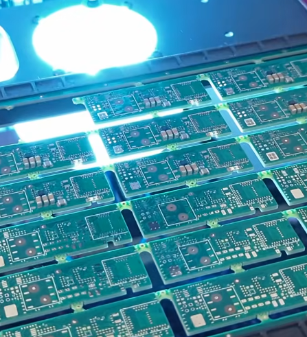
Depth camera mainboards are often space-constrained (e.g., inside handheld devices or compact robotic gimbals), typically utilizing HDI (High-Density Interconnect) multilayer board structures that incorporate microvias and any-layer interconnect technology.
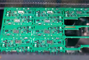
Fine-pitch component placement: The board hosts numerous ultra-fine-pitch BGAs, QFNs, and miniature connectors. We utilize high-end, high-precision placement equipment (ASM/Mycronic) to maintain placement accuracy within ±0.01 mm, ensuring precise pad alignment.
Precision reflow soldering temperature control: We use multi-zone reflow ovens with nitrogen protection to optimize temperature profiles. This prevents issues such as cold solder joints, bridging, and micro-cracks in components, while ensuring the uniform release of thermal stress across complex multilayer boards during the soldering process.
Optical alignment and active calibration processes
The essence of a depth camera lies in the integration of optics, mechanics, electronics, and computing; the parallelism and center alignment between the optical module and the sensor reference plane directly determine the camera’s calibration parameters.
High-Precision Active Alignment: High-precision optical adjustment equipment is introduced during the post-PCBA assembly stage. Through dynamic projection and image feedback, the six-axis spatial position (X, Y, Z, Pitch, Yaw, Roll) of the lens relative to the image sensor is adjusted in real-time to achieve optimal optical imaging and depth output.
Dust and Cleanliness Control: The entire optical PCBA assembly and lens module bonding process takes place in ISO Class 7 to Class 5 cleanrooms, preventing microscopic dust from entering the optical path and causing pixel-level noise or shadowing.
Thermal Design and Thermal Management Control
Depth processors (such as AI computing chips) and VCSELs generate significant heat during continuous operation; localized overheating can lead to increased sensor thermal noise, ranging drift, or even thermal shutdown.
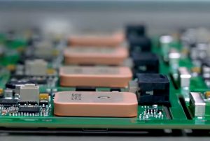
Thermal Path Optimization: The PCBA design extensively utilizes embedded copper blocks and high-density thermal via arrays, with high-performance thermal phase-change materials or thermal gels precisely applied to the back of key heat sources.
Structural Thermal Synergy: Metal housings and heat sinks are integrated to create a three-dimensional thermal dissipation loop—extending from the chip to the PCBA and finally to the housing—ensuring stable, long-term operation in harsh industrial environments ranging from -20°C to 60°C.
Quality Control System and Industry Standards
IPC-A-610 Class 3 Electronic Assembly Acceptance Standards
For high-end industrial, medical, and automotive-grade depth cameras, we strictly adhere to the IPC-A-610 Class 3 standard—the most rigorous international benchmark for electronic assembly acceptance. We enforce strict controls on solder joint fullness, conformal coating thickness, component cleanliness, and mechanical structural integrity to ensure products can withstand extreme vibration and shock.
IATF 16949 Quality Control for Automotive and Robotics Ecosystems
We strictly implement the IATF 16949 automotive quality management system throughout our quality management processes. We implement full-lifecycle quality traceability and closed-loop management, covering everything from supplier qualification audits and IQC (Incoming Quality Control), IPQC (In-Process Quality Control), AOI (Automated Optical Inspection), and SPI (Solder Paste Inspection) to X-ray non-destructive testing.
Reliability Testing for Harsh Environments
Every depth camera PCBA solution must pass rigorous reliability verification tests (EVT/DVT stages) before mass production:
High/Low-Temperature Cycling Test: Testing electrical performance and thermal stress under rapid temperature fluctuations ranging from -40°C to 85°C.
Vibration and Drop Tests: Simulating the frequent vibration scenarios found in automotive and industrial robotics applications to assess solder joint fatigue resistance.
Burn-in Testing: High-temperature, full-load aging screening to eliminate components prone to early-life failure, ensuring industry-leading MTBF (Mean Time Between Failures) metrics.
OEM/ODM Customization Services and Mass Production Delivery Process
Solution Assessment and Collaborative DFM/DFT Design
Professional Engineering Team Involvement: Upon receiving customer specifications—such as physical dimensions, field of view (FOV), operating range, interface type, and power consumption requirements—our team of senior hardware and structural engineers delivers a feasibility assessment report within 24 hours.
DFM (Design for Manufacturability) and DFT (Design for Testability): We optimize test points, panelization strategies, and routing specifications during the schematic and PCB layout phases. This proactive approach boosts yield rates, shortens lead times, and reduces overall BOM costs from the very beginning.
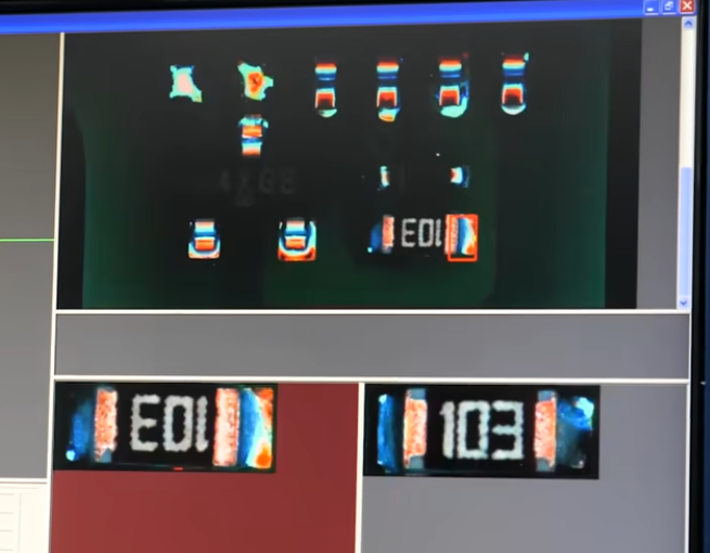
Prototype Fabrication and Integrated Optical/Electrical Debugging
Rapid Prototyping and Multifunctional Debugging: We offer expedited prototype delivery. Supported by professional optical laboratories and darkroom facilities, we facilitate the integrated debugging of depth map output, noise suppression, and calibration parameters (intrinsic/extrinsic matrices).
Firmware and Low-Level Driver Coordination: We assist customers in implementing UVC drivers, porting depth computation SDKs, and programming calibration data across Linux, Android, and RTOS platforms. Supply Chain Management and Agile, Flexible Mass Production Delivery
Directly Authorized Supply Chain: We maintain deep strategic partnerships with leading domestic and international component manufacturers and distributors (such as Sony, OmniVision, ams OSRAM, and ST). This ensures a stable supply of genuine core sensors and laser components, mitigating risks associated with supply shortages and price fluctuations.
Intelligent SMT Manufacturing Workshop: Leveraging modern high-speed SMT placement lines, fully automated dispensing systems, reflow soldering, and in-line inspection equipment, we enable seamless transitions from agile small-to-medium batch manufacturing to large-scale industrial mass production. We provide high-quality, one-stop OEM/ODM intelligent manufacturing services for depth cameras to global smart manufacturing enterprises.