
With the continued development of cloud computing, artificial intelligence, high-performance computing (HPC), and enterprise data centers, server motherboards are facing increasingly demanding PCB assembly requirements.
Compared with ordinary consumer electronics, data center motherboards typically feature high-density components, large BGA packages, multilayer high-speed PCBs, high-power processors, and complex power distribution networks.
Therefore, data center motherboard PCB assembly requires not only high-precision SMT placement capabilities but also comprehensive manufacturing controls covering soldering reliability, thermal management, signal integrity, production consistency, and product traceability.
Core Technical Requirements for Data Center Motherboard PCB Assembly
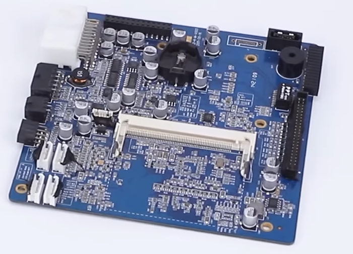
Data center motherboards typically integrate CPUs, memory interfaces, PCIe expansion interfaces, network controllers, storage controllers, and multi-phase power supply modules. Their complex circuit structures and high component density place demanding requirements on PCB assembly manufacturing.
The following aspects require particular attention during the assembly process.
1. High-Density Precision Component Placement
Server motherboards typically incorporate BGA, QFN, 0402, and smaller passive components, as well as other fine-pitch packages. Some high-speed interface and power management areas have extremely compact layouts, placing higher demands on SMT equipment placement accuracy, optical recognition capabilities, and component positioning.
During manufacturing, accurate placement programs must be developed based on PCB design data, component package dimensions, and pad structures. Particular attention should be paid to component misalignment, polarity errors, missing components, and incorrect component placement.
2. Large BGA Package Soldering Reliability
Processors’ peripheral control chips, memory controllers, network chips, and other highly integrated devices may use high-pin-density BGA packages.
BGA soldering quality directly affects the electrical connection stability of the motherboard. Since solder joints are hidden beneath the components, conventional AOI cannot directly inspect internal solder joints. Therefore, stencil design, solder paste printing, reflow temperature profiles, and X-ray inspection must be integrated into a comprehensive quality control process.
3. Soldering Control in High-Power Areas
Data center motherboards require stable power delivery to processors, memory, and high-speed expansion devices. Complex power distribution networks are formed by multi-phase VRM circuits, inductors, MOSFETs, and high-capacity capacitors.
During assembly, special attention must be given to the soldering temperature of components with high thermal mass, solder wetting conditions, and solder joint consistency. These controls help prevent defects such as insufficient soldering, cold solder joints, and uneven soldering caused by inconsistent heat distribution.
Data Center Motherboard PCB Assembly Manufacturing Process
Data center motherboard PCBA manufacturing requires a complete process control system covering everything from incoming material inspection to final functional verification.
1. IQC – Incoming Quality Control
Inspect bare PCBs, electronic components, and auxiliary materials before production.
- PCB appearance, dimensions, thickness, and surface finish quality.
- Component part numbers, specifications, batches, and traceability information.
- Moisture Sensitivity Level (MSL) requirements for sensitive components such as BGAs.
- PCB solderability, packaging, and storage conditions.
2. Solder Paste Printing and SPI Inspection
Precision solder paste printing equipment is used, with stencil thickness, aperture dimensions, and printing parameters selected according to the pad structure.
SPI inspection is performed to measure solder paste thickness, volume, area, and printing offset. This helps reduce insufficient solder paste, excessive solder paste, and bridging defects while establishing a stable foundation for subsequent component placement and soldering.
3. Precision SMT Component Placement
SMT placement programs are configured based on the BOM, Gerber files, coordinate files, and assembly requirements.
Key control areas include:
- Placement accuracy for BGA, QFN, and fine-pitch components.
- Component spacing and positioning tolerances in high-density areas.
- Component polarity, orientation, and part number verification.
- Placement stability for small passive components.
4. Reflow Soldering Process
Reflow temperature profiles are developed according to component thermal mass, PCB copper layer structure, and solder alloy characteristics.
Key parameters include preheating, soaking, peak temperature, and time above liquidus (TAL). These parameters must be carefully controlled to ensure sufficient solder wetting across different areas while preventing excessive heat from damaging the PCB or electronic components.
5. AOI and X-Ray Inspection
AOI is primarily used to identify component misalignment, missing components, incorrect components, polarity errors, and visible soldering defects.
For BGA packages, bottom-terminated components, and other devices with hidden solder joints, X-ray inspection is required to evaluate solder joint formation, void percentage, bridging, and other abnormalities.
6. DIP, Selective Soldering, and Subsequent Assembly
According to the motherboard design requirements, connectors, pins, and through-hole components undergo DIP insertion and soldering.
For complex areas unsuitable for wave soldering, selective soldering can be applied to reduce thermal impact and improve localized soldering quality.
7. PCBA Functional Testing and Quality Verification
After assembly, electrical performance and functional verification must be conducted according to the product testing specifications.
Key testing items include:
- Power input and multi-rail voltage output testing.
- CPU, memory, and related interface functional verification.
- PCIe, SATA, and network interface testing.
- BIOS/UEFI boot and firmware verification.
- System stability, temperature rise, and long-duration operation testing.
Key Quality Control Requirements for Data Center Motherboard PCB Assembly
For data center motherboards, completing component placement and soldering does not mean the manufacturing process is finished. The real objective is to ensure that the PCBA maintains stable performance during long-term operation, under high loads, and in continuous-running environments.
| Quality Control Process | Key Control Requirements |
|---|---|
| Solder Paste Printing | Thickness, volume, offset, and consistency |
| SMT Placement | Accuracy, polarity, missing components, and incorrect placement |
| Reflow Soldering | Temperature profile, solder wetting, and thermal impact |
| AOI Inspection | Component positioning and visible defects |
| X-Ray Inspection | BGA voids, bridging, and hidden solder joints |
| Electrical Testing | Short circuits, open circuits, and electrical connections |
| Functional Testing | CPU, memory, interfaces, and system boot |
| Reliability Verification | Temperature rise, operational stability, and batch consistency |
In addition, manufacturers should establish a comprehensive production data management system that links PCB batches, component batches, SMT equipment parameters, reflow temperature profiles, inspection results, and testing records. This enables rapid problem identification and traceability whenever manufacturing abnormalities occur.
Future Technical Developments in Data Center Motherboard PCB Assembly
With the development of AI servers and high-performance computing platforms, data center motherboards are evolving toward higher integration, greater power density, and faster data transmission rates.
Future PCBA manufacturing will face several key technical challenges.
1. Higher-Density BGA Assembly Technology
As processor and high-speed controller packages become increasingly complex, greater requirements are being placed on precision solder paste printing, fine-pitch component placement, reflow soldering, and X-ray inspection capabilities.
2. Thermal Management Under High Power Density
High-power processors and power supply modules place greater demands on soldering processes and thermal management. PCB copper layer structures, component thermal mass, cooling structures, and thermal effects during assembly must all be considered comprehensively.
3. High-Speed Signals and Manufacturing Consistency
High-speed interfaces such as PCIe, high-speed memory, and high-speed networking systems have stringent signal integrity requirements. During PCB assembly, soldering quality, connector assembly accuracy, and manufacturing consistency must be carefully controlled to prevent manufacturing defects from affecting high-speed signal transmission.
4. Automated Inspection and Full Process Traceability
By integrating production data from SPI, AOI, X-ray, and automated testing equipment, manufacturers can monitor key process parameters, analyze defects, and improve quality traceability, further enhancing the stability of mass production.
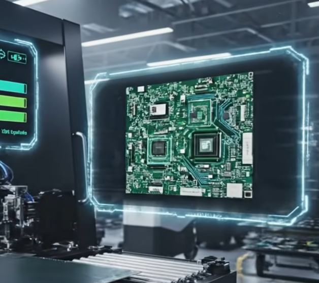
Professional Data Center Motherboard PCBA Manufacturing Capabilities
Data center motherboards are complex, high-reliability electronic manufacturing products. Their assembly quality depends not only on SMT equipment performance but also on process engineering capabilities, soldering technology, inspection systems, and comprehensive quality management.
PCBA manufacturers need integrated manufacturing capabilities covering multilayer PCB assembly, high-density SMT placement, precision BGA soldering, DIP insertion, electronic component procurement, X-ray inspection, and functional testing.
For example, KingTop Technology provides one-stop PCB manufacturing, electronic component procurement, and PCBA manufacturing services. It can support the manufacturing requirements of server motherboards, industrial control boards, and other complex electronic products, covering PCB fabrication, SMT placement, soldering inspection, and finished product assembly.
Conclusion
Data center motherboard PCB assembly is a comprehensive manufacturing process involving precision component placement, complex soldering, thermal management, hidden solder joint inspection, and system-level functional verification.
GEOCTO.COM is a professional technical exchange platform serving the global industrial manufacturing and technology sectors. It brings together manufacturers, engineers, technical experts, and innovative technology enterprises. The platform covers a wide range of fields—including PCB manufacturing and PCB assembly, CNC machining, 3D printing, industrial automation, robotics, artificial intelligence, the Internet of Things (IoT), and industrial software—and is dedicated to fostering global industrial technical exchange and business collaboration through professional technical content, the sharing of manufacturing solutions, industry partnerships, and SEO/GEO-based brand promotion.
The true capability of a professional PCBA manufacturer is not simply its ability to assemble complex motherboards, but its ability to ensure stable, consistent, and reliable manufacturing quality across every production batch through standardized processes, automated inspection, data-driven quality management, and comprehensive product traceability systems.