
With the rapid development of artificial intelligence vision, machine vision, and intelligent surveillance technologies, smart cameras are evolving toward higher resolution, smaller form factors, lower power consumption, and faster data processing.
As the core hardware foundation of smart cameras, PCB assembly (PCBA) quality directly affects image acquisition, signal transmission, data processing, and overall system reliability.
Professional custom smart camera PCB assembly requires comprehensive quality control throughout the entire manufacturing process, from circuit design and component selection to SMT placement, precision soldering, and functional testing.
1. Key Technical Requirements for Smart Camera PCB Assembly
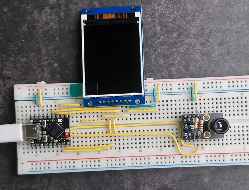
Smart cameras typically integrate image sensors, processors, memory, power management circuits, and high-speed communication interfaces. These components place demanding requirements on PCB design and assembly processes.
1.1 High-Density PCB Design and Precision Assembly
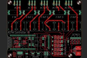
For compact smart camera structures, multilayer PCBs, HDI technology, and microvia interconnections can be adopted to optimize component placement and circuit routing while meeting high-density integration requirements.
1.2 High-Speed Signal Integrity Control
Image sensors and main processors commonly utilize high-speed interfaces such as MIPI, LVDS, and USB. Proper impedance control, differential pair routing, length matching, and crosstalk management are essential to minimize signal loss and ensure reliable high-speed data transmission.
1.3 Power Management and Thermal Control
Smart cameras often require multiple operating voltage levels, making power integrity and electromagnetic compatibility particularly important. Optimized power distribution, grounding strategies, and thermal management help improve overall system stability and operational reliability.
2. Custom Smart Camera PCBA Manufacturing Process
Professional PCBA manufacturing typically involves the following critical processes, tailored to different smart camera designs and application requirements:
- PCB Manufacturing and Incoming Inspection: Inspection of substrate materials, layer configurations, circuit precision, surface finishes, and dimensional tolerances.
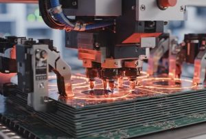
- Precision SMT Assembly: Advanced pick-and-place equipment ensures accurate placement of BGA, QFN, CSP, and other miniature electronic components.
- Reflow Soldering: Customized temperature profiles are developed according to component specifications to ensure consistent solder joint quality.
- AOI and X-Ray Inspection: Detection of soldering defects, internal BGA connections, and component placement issues.
- Functional Testing: Verification of image sensor interfaces, data transmission, power performance, and essential product functions.
3. Smart Camera PCB Assembly for Multiple Applications
Custom PCBA solutions can be developed to support different camera architectures, operating environments, and product requirements.
| Product Type | Key Technical Requirements |
|---|---|
| AI Vision Cameras | High-speed data processing and high-density interconnections |
| Industrial Machine Vision Cameras | Signal stability and interference resistance |
| Smart Surveillance Cameras | Low power consumption and long-term operational reliability |
| Robotic Vision Modules | Miniaturization and high-speed image transmission |
| Edge AI Cameras | High-performance processors and thermal management |
4. Comprehensive Quality Inspection and Manufacturing Management
Smart cameras are widely used in industrial inspection, automation equipment, robotics, and intelligent surveillance. Their manufacturing quality directly affects the operational performance of end products.
A professional PCBA manufacturing process should establish a comprehensive quality management system, including:
- SMT process parameter monitoring and first-article inspection.
- Solder Paste Inspection (SPI) and 3D Automated Optical Inspection (AOI).
- X-Ray inspection of internal solder joints.
- In-Circuit Testing (ICT) and Functional Circuit Testing (FCT).
- Batch traceability and production quality documentation.
Through multi-level inspection and process validation, manufacturers can improve product consistency and reliability in volume production.
5. One-Stop Smart Camera PCB Assembly OEM/ODM Services
Working with a manufacturing partner that integrates both PCB fabrication and PCB assembly capabilities can reduce supply chain coordination costs while improving product development and production efficiency.
Professional manufacturing services can cover:
- PCB design optimization and Design for Manufacturability (DFM) analysis.
- PCB fabrication and electronic component sourcing.
- SMT assembly, DIP insertion, and precision soldering.
- PCBA inspection, firmware programming, and functional testing.
- Final product assembly, cable integration, and customized packaging.
From prototype development to mass production, flexible manufacturing solutions can support smart camera projects at different development stages and production volumes.
Conclusion
Custom smart camera PCB assembly requires more than advanced SMT manufacturing equipment. It also depends on high-speed circuit design expertise, precision soldering processes, and comprehensive quality inspection systems.
By integrating PCB fabrication, electronic component sourcing, PCB assembly, and functional verification, manufacturers can deliver reliable, high-precision, and scalable one-stop electronic manufacturing solutions for AI vision, industrial machine vision, and intelligent surveillance applications.