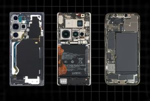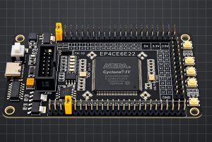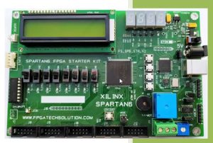

As AI computing power continues to extend toward the edge, workstations, and data centers, the demands placed on PCBs by GPUs, NPUs, AI accelerator cards, high-speed network modules, and edge inference devices have grown significantly.
With the continuous increase in chip package pin counts, the shrinking of BGA (Ball Grid Array) pitch, and the rise in high-speed interface data rates, both power supply current and thermal density have intensified. Traditional multilayer PCBs are increasingly strained in terms of routing space, interconnect length, and power distribution.
HDI (High-Density Interconnect) technology enhances interconnect capacity per unit area through the use of micro-vias (blind and buried vias), fine-line circuitry, and sequential build-up manufacturing. This provides greater flexibility for package fan-out and routing space for AI chips with high pin densities. HDI assembly encompasses board-level design, material selection, micro-via reliability, precision SMT (Surface Mount Technology), thermal management, and system verification.
I. Why AI Hardware Requires HDI Technology
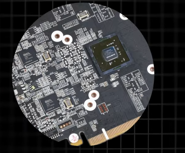
The core characteristic of AI hardware is the concentration of high-performance computing chips, high-speed memory, high-speed interconnects, and high-power supply components within a limited space. GPUs, NPUs, FPGAs, and custom AI ASICs typically utilize high-pin-count BGAs or advanced packaging, requiring the placement of DDR, LPDDR, or HBM interfaces, power management components, clock circuitry, and high-speed transceiver channels around the chip.
When pin pitch is small, conventional through-holes consume space across multiple routing layers, making it difficult to achieve effective fan-out between chip pads. HDI technology utilizes laser-drilled micro-vias to connect adjacent or specific conductive layers, reducing the space occupied by through-holes, increasing routing density, and freeing up room for ground planes, power planes, and high-speed signal layers.
In AI hardware, HDI offers value in three primary areas:
First, it enhances package fan-out capability. Micro-vias, blind vias, and buried vias support high-density pin connections for components such as fine-pitch BGAs and CSPs (Chip Scale Packages), thereby reducing routing congestion.
Second, it optimizes high-speed interconnects. Proper planning of the layer stack-up and via structure can reduce parasitic parameters introduced by signal layer transitions, while improving impedance continuity, crosstalk, and signal loss.
Third, HDI enhances system integration. Within the same physical footprint, HDI technology facilitates the integration of additional memory, power management, networking, and control circuitry—making it well-suited for space-constrained AI edge devices and high-performance computing boards.
It should be noted that HDI is not a mandatory requirement for all AI products. If the chip I/O density, board area, and routing complexity are relatively low, conventional multi-layer PCBs may be more cost-effective. The choice should be based on a comprehensive assessment of factors such as package escape routing capabilities, layer count, interface data rates, power consumption, and cost.
II. HDI Structure and Microvia Design
Common HDI structures include 1-stage, 2-stage, and Any-Layer Interconnect (ALIC) configurations. Typical build-up structures include 1+N+1, 2+N+2, and similar formats; the specific number of layers and stages should be determined by routing requirements, board thickness, via diameter, material systems, and manufacturing capabilities.
A 1+N+1 structure typically adds one build-up layer on each side of the core board, making it suitable for medium-density pin fan-outs. A 2+N+2 structure provides more microvia connections and routing space, catering to higher-density components. Any-Layer Interconnect allows for microvia connections between any layers, though it entails greater process complexity and higher costs.
Microvia design requires careful control of via diameter, dielectric thickness, aspect ratio, copper plating quality, and pad dimensions. Smaller is not necessarily better; via diameter, copper thickness, dielectric thickness, and alignment precision must all fall within the supplier’s stable process window. Designers must also evaluate microvia landing positions, pad capture capabilities, and manufacturing tolerances between adjacent structures.
For fine-pitch BGA components, common approaches include “dog-bone” fan-outs, Via-in-Pad (VIP) designs, and laser microvia fan-outs. Via-in-Pad designs help save routing space but typically require via filling, plating, and surface planarization processes. If a stacked-via structure is adopted, the interfaces between microvias and the reliability under thermal cycling must be specifically validated. Whenever the design permits, a staggered-via structure is generally preferable, as it helps reduce stress concentration at continuous interfaces. One should not blindly opt for stacked vias solely to minimize the number of layers.
III. PCB Stack-up Design for AI Chips
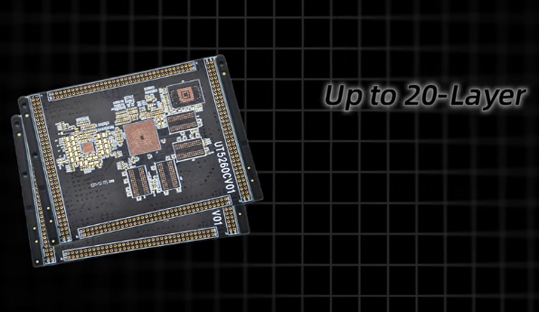
The stack-up design determines both the electrical performance and the manufacturability of an HDI (High-Density Interconnect) board. AI accelerator boards typically incorporate high-speed signal layers, ground reference layers, power distribution layers, and low-speed control layers. It is essential to first identify critical nets before planning the relationships between layers.
For high-speed differential signals, it is crucial to maintain a continuous reference plane, while controlling differential and single-ended impedance, trace width and spacing, and return paths. Interfaces such as PCIe, Ethernet, SerDes, and high-speed memory require simulations that account for actual data rates, channel lengths, and device specifications. Via-based layer transitions introduce parasitic capacitance, inductance, and impedance discontinuities; where necessary, techniques such as back-drilling, optimizing pad and anti-pad dimensions, and minimizing unnecessary via transitions should be employed.
For DDR and other parallel memory buses, focus must be placed on topology, timing, length matching, and crosstalk constraints. Differential clocks require careful control of symmetry, reference plane integrity, and proximity to noise sources. Length matching must also account for propagation delays, interlayer dielectric properties, and variations in package-level routing.
Power integrity (PI) is another critical aspect of AI hardware design. GPUs and NPUs generate transient currents during rapid load fluctuations; therefore, the power delivery network (PDN) must be designed to manage DC voltage drop, AC impedance, and transient response. The design should align with the chip manufacturer’s power supply requirements—optimizing power planes, copper thickness, supply paths, and the placement and capacitance values of decoupling capacitors—while also verifying the loop inductance between the chip’s power pins and the capacitors.
HDI stack-up design must balance signal integrity (SI), power integrity (PI), electromagnetic compatibility (EMC), and thermal considerations.
IV. Material and Manufacturing Process Control
AI hardware is highly sensitive to factors such as high-speed signal loss, dimensional stability, and thermal reliability. Material selection should take into account signal frequency, board thickness, copper thickness, operating temperature, and cost, while evaluating the dielectric constant (Dk), dissipation factor (Df), moisture absorption, and coefficient of thermal expansion (CTE).
High-speed channels may require low-loss or ultra-low-loss materials, whereas high-power areas necessitate a focus on the substrate’s heat resistance, the type of copper foil used, and thermal conduction paths. When using a hybrid stack-up (mixing different materials), it is essential to verify differences in thermal expansion, lamination process windows, and the risk of board warpage.
HDI (High-Density Interconnect) manufacturing involves processes such as inner-layer circuit fabrication, lamination, laser drilling, via metallization, electroplating, and surface finishing. During multi-stage sequential lamination, factors such as inter-layer registration, the cleanliness of the bottom of microvias, the continuity of copper plating within vias, and dielectric thickness all influence the final reliability of the board.
Key control points include: ensuring no resin residue or contaminants remain at the bottom of microvias, which could impede electrical connectivity; ensuring that copper plating within vias is continuous and uniform, free from voids, cracks, or thin-copper areas; verifying trace width, spacing, and the absence of notches after circuit etching; and controlling board thickness, inter-layer bonding, and warpage after lamination. Before mass production, high-density boards must undergo cross-sectional analysis, via copper integrity checks, impedance testing, and necessary thermal stress validation.
V. SMT Process Considerations for HDI Board Assembly
While HDI substrates are highly complex to manufacture, the quality of the final product also depends on the PCBA (Printed Circuit Board Assembly) process. Boards for AI chips often integrate large-format BGAs, fine-pitch components, high-pin-count connectors, and a large number of decoupling capacitors; therefore, placement accuracy, solder paste printing, and reflow soldering profiles must be strictly controlled.
Incoming Material and Moisture Sensitivity Management
Prior to assembly, verify the PCB revision, thickness, surface finish, physical appearance, pad quality, and critical dimensions. For moisture-sensitive components, manage the opening, storage, baking, and floor-life (exposure time) based on their specific Moisture Sensitivity Level (MSL) and packaging status. PCBs themselves must also be stored in a moisture-controlled environment—following the requirements of the material manufacturer and supplier—to prevent moisture-induced issues during reflow, such as delamination, “popcorning” (internal board explosion), or soldering defects.
Stencil Design and Solder Paste Printing
Fine-pitch BGAs and miniature passive components are highly sensitive to stencil aperture design, thickness, paste release characteristics, and solder paste particle size. Stencil design must strike a balance between achieving the required solder joint volume and minimizing the risk of bridging. Post-printing Solder Paste Inspection (SPI) is essential to verify the area, height, volume, and alignment of the deposited paste, allowing for the early detection of insufficient or excessive solder, missing deposits, or positional inaccuracies before component placement.
High-Precision Placement
BGAs, CSPs, and fine-pitch components require placement equipment with robust vision recognition, precise positioning, and accurate pressure control. Placement data must be strictly aligned with PCB coordinates, component packaging specifications, and polarity requirements. For large-scale AI chips, it is also critical to account for the coplanarity between the chip, PCB, and fixture, as well as differences in thermal expansion, to prevent localized stress or placement offsets.
Reflow Soldering Window
The reflow profile must be developed based on solder paste specifications, component temperature tolerances, the thermal capacity of the PCB, and the thermal distribution across the board. Parameters such as the heating rate, soak time, peak temperature, and cooling rate should be verified through empirical measurements using thermocouples. Since large chips and areas with thick copper layers can easily develop temperature differentials, process quality cannot be assessed solely based on the reflow oven’s set temperature values.
Post-Soldering Inspection
Automated Optical Inspection (AOI) is used to verify solder joints, component polarity, and the presence of all components. For BGA components, X-ray inspection is required to check for voids, bridging, and alignment issues. For high-value computing boards, additional testing methods—such as In-Circuit Testing (ICT), boundary scan, flying-probe testing, or functional testing—may be implemented based on risk assessment. The inspection strategy should comprehensively cover all critical failure modes.
VI. Thermal Management and Mechanical Reliability
Given the high power consumption and significant heat flux density of AI chips, PCB assembly must be designed in tandem with the thermal management structure. Heat is typically dissipated through a conduction path that includes the chip package, solder pads, PCB copper layers, thermal vias, and a heatsink or cold plate. For high-power components, the design must incorporate thermal pads, copper planes, and arrays of thermal vias—tailored to the specific requirements of the chip package—while ensuring adequate heat spreading capability.
More thermal vias do not necessarily equate to better performance; factors such as via diameter, pitch, filling method, the risk of solder wicking, and inter-layer reliability must all be carefully considered. When using via-in-pad designs, it is essential to control the quality of the via-filling process and the flatness of the surface to prevent solder paste loss and the formation of voids in solder joints. If thermal interface materials, clamping mechanisms, or liquid-cooling cold plates are employed, one must also evaluate whether the assembly pressure could cause PCB warpage, fatigue in BGA solder joints, or excessive mechanical stress on components.
Regarding mechanical reliability, large-format boards, heavy heatsinks, and high-mass connectors can introduce flexural stress. The layout of mounting holes, support points, connectors, and local copper distribution should be optimized accordingly. Testing protocols—including high/low-temperature cycling, thermal shock, vibration, and long-term powered operation—should be defined based on the product’s intended operating environment and required reliability grade.
VII. Quality Inspection and Reliability Verification
Quality control for HDI (High-Density Interconnect) board assemblies must encompass three levels: the bare PCB, the SMT (Surface Mount Technology) assembly process, and the functionality of the complete system.
At the bare PCB stage, the focus is on verifying microvia continuity, the integrity of copper plating within vias, interlayer connections, trace dimensions, impedance, board thickness, and warpage. Where necessary, structural reliability should be validated through cross-sectioning, thermal stress testing, insulation resistance testing, and withstand voltage testing. During the assembly phase, attention should be directed toward solder paste printing, component placement accuracy, reflow profiles, BGA solder joint integrity, and cleanliness. At the functional stage, checks should cover power-on sequencing, power supply ripple, critical power rails, clock signals, memory training, high-speed link integrity, and the stability of the system under AI computational loads.
For AI accelerator cards, it is recommended to establish a comprehensive test flow—from the individual board level to the full system level. This begins with short-circuit checks and current-limited power-on, followed by the verification of power rails and boot sequences. Subsequently, the process should include memory initialization, high-speed interface link training, stress-testing of computational workloads, and long-duration full-load testing. Throughout these tests, parameters such as temperature, current, error logs, and performance fluctuations should be monitored to identify intermittent faults or heat-related failures that might not be detectable through visual inspection alone.
Quality standards should be clearly defined during the early stages of a project. Soldering processes may be governed by the IPC J-STD-001 standard, while the acceptance of electronic assemblies may follow IPC-A-610. Specific versions and acceptance criteria should be determined based on the product’s reliability class, customer specifications, and contractual agreements.
For the design, manufacturing, and performance requirements of bare HDI (High-Density Interconnect) boards, one should apply IPC design and performance standards that correspond to the specific board type and structure; assembly acceptance criteria must not be conflated with bare-board manufacturing standards.
VIII. Engineering Collaboration for HDI-Based AI Hardware Projects
A common risk in HDI projects is the lack of early-stage collaboration between design teams, PCB fabricators, and PCB assembly providers. For instance, a design might specify micro-via dimensions that exceed a fabricator’s stable process capabilities, potentially compromising the reliability of subsequent reflow soldering. Alternatively, inconsistencies between chip packaging, stencils, and pad definitions can result in an overly narrow process window for BGA soldering.
It is recommended to conduct DFM (Design for Manufacturing), DFA (Design for Assembly), and DFT (Design for Testability) reviews before the design is frozen. DFM reviews should focus on trace width/spacing, via diameters, stacked-via structures, board thickness, and materials. DFA reviews should address component spacing, pad design, stencils, component orientation, thermal management structures, and space for rework. DFT reviews should involve early planning for test points, boundary scan capabilities, and functional test interfaces.
Version control must be strictly maintained for all design and manufacturing data, including Gerber or ODB++ files, drill files, BOMs, component coordinate files, assembly drawings, stencil designs, and test programs. For critical chips and specialized materials, it is also necessary to manage supply chain batches, the approval of alternative components, and traceability records.
IX. Application Scenarios and Selection Guidelines for HDI Board Assembly
HDI technology is well-suited for AI hardware that demands high interconnect density, compact form factors, and superior electrical performance. Applications include GPU computing modules, NPU acceleration cards, AI edge computing terminals, machine vision controllers, main control boards for intelligent robots, high-speed communication modules, and high-density storage control boards.
When selecting an HDI solution, one should look beyond simple metrics like layer count or trace width; it is essential to evaluate factors such as chip escape routing, interface data rates, power consumption, current requirements, thermal management, physical dimensions, production volume, and cost. During the prototyping phase, priority should be given to validating critical signal paths, power delivery, and thermal design. In the pilot production phase, the focus should shift to verifying manufacturing process windows, soldering yields, and test coverage.
During mass production, continuous monitoring is required for micro-via quality, board warpage, reflow profiles, BGA defect rates, and long-term reliability. When evaluating suppliers, key factors to consider include their HDI (High-Density Interconnect) tier capabilities, laser drilling and sequential lamination processes, microvia reliability data, impedance control, material management, precision SMT equipment, and X-ray inspection capabilities. Equally important is the supplier’s ability to participate in early-stage engineering reviews and provide actionable process feedback.
Conclusion
The assembly of HDI (High-Density Interconnect) boards serves as a critical engineering foundation for AI hardware, enabling high integration, high-speed communication, and stable power delivery. Ultimately, product competitiveness is not defined merely by finer circuitry or a higher density of microvias; rather, it stems from seamless, end-to-end collaboration—spanning chip packaging, PCB stack-up design, material fabrication, SMT assembly, thermal management, and system-level verification.
As a technical service provider in the PCB manufacturing and assembly sector, KingTop Technology focuses on the deep integration of HDI technology with the specific requirements of AI hardware manufacturing. We are dedicated to providing PCB fabrication, precision assembly, and engineering support for high-performance computing devices, AI accelerator cards, and intelligent hardware—helping our clients navigate the challenges of complex circuit design, high-precision manufacturing, and high-reliability assembly.
For AI accelerator cards and edge AI devices, the high-density advantages of HDI can only be translated into stable, mass-producible hardware performance when manufacturability is prioritized during the design phase, precision soldering and process windows are strictly controlled during assembly, and a closed-loop system is established through electrical, thermal, and reliability testing. KingTop Technology remains committed to advancing HDI PCB manufacturing and PCB assembly processes, supporting AI hardware products from initial engineering design through to full-scale mass production.