
Testing the communication between an FPGA and an SD card serves not only to verify data read/write functionality but also acts as a critical method for evaluating digital interface timing, power integrity, PCB routing quality, and the reliability of the electronic assembly.
For applications such as embedded control, industrial data acquisition, image processing, and high-speed data logging, a well-designed and thoroughly tested communication board can significantly shorten the hardware debugging cycle, providing a solid foundation for subsequent product development and mass production.
I. Design Objectives for FPGA-to-SD Card Communication Testing
A PCB designed for FPGA-to-SD card communication testing typically consists of an FPGA controller, power management circuitry, an SD card interface, configuration and debugging ports, and specialized test circuitry. The FPGA handles the communication control logic, while the SD card is used to store test data, configuration files, or acquisition results. Peripheral circuits ensure proper power supply, electrical compatibility, and reliable signal transmission.
In practical engineering, the design objectives should extend beyond simply achieving a successful read/write operation; they should encompass the following key capabilities:
Communication Functionality Verification: Ensuring proper SD card initialization, command response, data read/write operations, and error handling.
Timing and Signal Verification: Evaluating the signal quality of clock, command, and data lines to minimize the risk of sampling errors.
Hardware Reliability Verification: Assessing power supply stability, card-insertion detection, electrostatic discharge (ESD) protection, and soldering quality.
Manufacturing Consistency Verification: Ensuring that test results remain reproducible across different PCB batches, various SD cards, and diverse operating conditions.
Consequently, circuit design, PCB layout, assembly processes, and testing strategies should be planned concurrently during the early stages of a project, rather than attempting to address issues retroactively after the prototype has been assembled.
II. SD Card Interface Schemes and Electrical Design
Selecting an Appropriate Communication Mode
Common communication modes for SD cards include SPI mode, 1-bit SD mode, and 4-bit SD mode. These modes differ in terms of control logic complexity, pin requirements, and data throughput capacity. The SPI mode interface is relatively simple, making it suitable for early-stage functional verification and basic read/write testing. The 1-bit SD mode reduces the number of data lines required, while the 4-bit SD mode utilizes data lines DAT0 through DAT3 for parallel transmission, which is better suited for storage testing that demands higher throughput.
When selecting a design approach, one should comprehensively consider factors such as available FPGA logic resources, the specific type of SD card, required data rates, the availability of controller IP, and the overall development timeline. If the project may require higher transmission performance in the future, it is advisable to incorporate a 4-bit interface and necessary debugging capabilities into the initial design.
It is important to note that SD card communication involves more than just simple GPIO-style level toggling. The FPGA must implement the corresponding protocol control logic, including initialization, command transmission, response reception, data transfer, and state management. If using an off-the-shelf controller IP, verify that it supports the required protocol modes, card capacities, clock frequency ranges, and error-handling mechanisms.
Power Supply and Voltage-Level Compatibility
The power supply for the SD card and the I/O voltage of the FPGA must be designed in strict accordance with the specifications of the chosen devices and the SD interface standard. One cannot assume interface compatibility based solely on the FPGA’s core voltage, nor should it be assumed that all FPGA I/O pins support 3.3V signaling.
During the schematic design phase, carefully verify the supply voltage of the FPGA’s I/O bank, the I/O standards, the pin tolerance specifications, and the electrical requirements of the SD card interface. If the voltage levels are incompatible, evaluate the use of an appropriate level shifter, ensuring it supports bidirectional data transmission, the required timing, and the necessary operating voltage.
The SD card power supply must be stable and capable of providing sufficient current. It is recommended to place appropriate decoupling capacitors near the power pins of the SD card slot; furthermore, the power supply’s transient response should be evaluated against current fluctuations that occur during card insertion, initialization, and continuous read/write operations.
For designs with stringent power integrity requirements, one should also examine factors such as voltage regulator output ripple, voltage drops along the power path, ground return paths, and the impact of dynamic load changes on the FPGA. This helps prevent initialization failures or intermittent communication errors caused by power supply irregularities.
Pull-up Resistors, Series Resistors, and ESD Protection
The configuration of pull-up resistors for CMD and DAT signals should be determined based on the specific SD communication mode in use, the controller documentation, and the SD interface standard. An excessively large pull-up resistor may adversely affect the signal rise time, while one that is too small can increase power consumption or alter the load on the driver; therefore, fixed values used in other projects should not be applied indiscriminately.
For CLK, CMD, and DATA signals, it is advisable to include pads for series resistors—factoring in drive capability, trace length, and edge characteristics—to allow for signal quality optimization during the prototype debugging phase. The specific resistance values should be determined based on device datasheets, signal integrity analysis, and empirical measurements, rather than being treated as a mandatory configuration for all SD card interfaces.
As an externally accessible interface, an SD card slot is susceptible to electrostatic discharge (ESD) and disturbances during insertion or removal. Designers should evaluate low-capacitance ESD protection devices and place them as close to the interface as possible to minimize the exposed path between the protected traces and the external connector.
Furthermore, the mechanical mounting of the card slot, power supply contacts, and card-detection circuitry must be verified. For applications requiring hot-plugging support, the design should also incorporate FPGA logic to handle card insertion detection, initialization retries, unexpected removal, and file system protection, thereby preventing erroneous write operations during card removal.
III. PCB Layout and Signal Integrity Design
Interface Layout and Component Placement
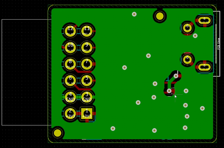
SD card slots are typically positioned near the edge of the PCB to facilitate card insertion/removal, mechanical assembly, and production testing. The placement of the FPGA and its associated control circuitry should be determined based on pin assignments, routing resources, and the overall layout, with the goal of minimizing the length of critical connections between the SD interface and the controller.
Power converters, switching nodes, and high-current loops should be kept at an appropriate distance from sensitive signals to prevent switching noise from coupling directly into the SD clock and data lines.
ESD protection devices should be located near the interface, and decoupling capacitors should be placed close to their respective power pins. When incorporating test points, one must balance ease of probing with the impact on signal loading, ensuring that the addition of test points does not introduce excessively long stubs or significant parasitic capacitance.
Routing of Clock, Command, and Data Lines
In an SD interface, the CLK signal serves as a critical timing reference. Clock edges, propagation delays, and data sampling windows all directly influence communication reliability.
During PCB routing, priority should be given to maintaining a continuous reference ground plane, ensuring that signals do not cross gaps in the ground or power planes. For CLK, CMD, and DAT lines, avoid unnecessary vias, long stubs, and abrupt impedance changes; evaluate trace lengths and signal integrity in the context of the target operating frequency.
In 4-bit mode, the timing relationships between data lines, as well as between the data lines and the clock, must be incorporated into constraint management. Length-matching requirements should not be defined in isolation; rather, they must be determined based on the specific controller, card slot architecture, target data rate, device design guidelines, and the actual timing budget.
FPGA pin assignment should also be completed during the early stages of layout. Proper planning of I/O banks, voltage standards, pin locations, and signal grouping can help minimize routing conflicts and reduce the risk of redesigns necessitated by subsequent pin adjustments.
PCB Stack-up and Return Paths
For a test board incorporating an FPGA, configuration memory, and an SD card interface, the number of PCB layers should be determined based on device packaging, routing density, power supply requirements, and manufacturing capabilities.
While a multi-layer PCB offers a more continuous reference plane and more efficient power distribution, a higher layer count is not necessarily better. Designers must strike a balance between cost, routing space, manufacturing precision, and electrical performance.
If the FPGA uses a BGA package, factors such as pad fan-out, via structures, pad pitch, and manufacturing process capabilities must be considered collectively. For high-density designs, it is essential to verify the manufacturer’s specific production parameters—such as minimum trace width, trace spacing, via diameter, annular ring width, and solder mask dam—during the layout phase to prevent issues where the design proves impossible to manufacture reliably.
IV. Quality Control for PCB Assembly and Manufacturing
FPGA Soldering and Assembly Process
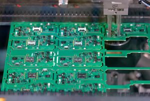
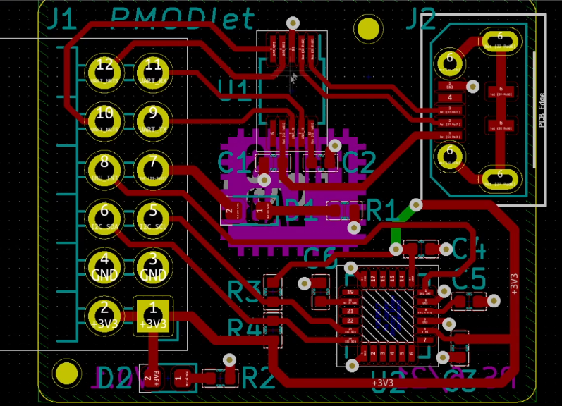
FPGAs may utilize packages such as fine-pitch QFP or BGA; the quality of their soldering directly impacts communication test results. For BGA components, since solder joints are located beneath the package—making it impossible to fully verify internal connections via visual inspection—quality assessment must integrate the placement process, reflow soldering parameters, and necessary X-ray inspection.
Prior to assembly, verify the PCB pad design, stencil aperture design, solder paste type, component solderability, and storage conditions. For moisture-sensitive components, implement moisture-control measures in accordance with the manufacturer’s specifications to prevent package damage during reflow soldering.
The reflow soldering temperature profile must be optimized based on the PCB’s thermal capacity, the FPGA package type, solder paste specifications, and the temperature tolerance of the components. A temperature profile used for a different product should not be directly applied to the current project.
Assembly of SD Card Slots and Peripheral Components
The assembly of SD card slots focuses not only on electrical solder joints but also on mechanical strength, insertion/extraction durability, and structural reliability.
During assembly, inspect the card slot’s solder pins, mounting pads, placement accuracy, and chassis-grounding design. If a card slot is subject to significant mechanical stress, ensure that pad dimensions, mounting methods, and local PCB support are appropriate for the component’s structure; this helps mitigate solder joint fatigue or pad damage caused by repeated insertion and extraction.
For ESD protection devices, series resistors, level shifters, and power supply capacitors, verify component orientation, package specifications, and soldering quality against the Bill of Materials (BOM).
It is recommended to incorporate test points on the PCB for critical debugging nodes and to include clear silkscreen markings for key components and interfaces, facilitating production inspection, troubleshooting, and future maintenance.

Design for Manufacturing (DFM) Assessment
Before initiating PCB production, a Design for Manufacturing (DFM) review must be completed. Key aspects to verify include the alignment between pads and stencil apertures, solder mask clearances, component spacing, the relationship between vias and pads, keep-out zones near board edges, and the mechanical dimensions of connectors.
Furthermore, version control must be applied consistently across schematic diagrams, PCB files, BOMs, coordinate files, stencil data, and assembly drawings. Any modifications—whether involving FPGA pins, SD card interface circuitry, or resistance/capacitance values—must undergo formal version verification to ensure that design files remain aligned with the actual production configuration.
For test boards, it is advisable to include dedicated interfaces for FPGA configuration, JTAG debugging, UART log output, and power supply measurement. Where necessary, incorporate provisions for independent power enabling or current monitoring to facilitate the rapid isolation of logic faults, power supply issues, or electrical anomalies at the interfaces.
V. Testing Procedure for FPGA-to-SD Card Communication
Once PCB assembly is complete, testing should proceed systematically, starting with basic electrical checks and advancing to full-scale communication verification.
Step 1: Pre-power-up Inspection.
Inspect the PCB for physical defects, component polarity, soldering quality, and the status of all interfaces. Measure the resistance to ground for all primary power rails to rule out any obvious short circuits. Pay particular attention to the FPGA power supply, I/O bank supply rails, and the SD card power supply.
Step 2: Initial Power-up and FPGA Configuration.
Verify that all supply voltages, power-up sequences, and current levels fall within the expected ranges. Subsequently, load the test logic via JTAG or the designated configuration interface. Confirm the configuration status, clock operation, and any relevant serial port logs.
Step 3: SD Card Initialization.
Insert an SD card that meets the design specifications. The FPGA controller should execute the initialization sequence, followed by a check of command responses, card identification data, and the initialization status. If initialization fails, prioritize troubleshooting the power supply, voltage-level compatibility, pull-up configurations, clock signals, and pin mapping.
Step 4: Single-block and Multi-block Read/Write Testing.
Begin by performing single-block data read/write operations, then proceed to continuous multi-block testing. Use fixed, incremental, or pseudo-random test data to verify data integrity and the accuracy of the control logic.
Step 5: Continuous Operation and Exception Testing.
Conduct stress tests—including cyclic read/write operations, extended continuous operation, repeated power cycling, and frequent card insertion/removal—to monitor for issues such as timeouts, CRC errors, data inconsistencies, or failures in card re-identification.
For products that support hot-swapping, also verify the system’s handling logic in the event of an unexpected card removal. Test results should document the SD card model, communication mode, operating clock frequency, data volume, error count, environmental conditions, and firmware version. Retaining reproducible test data is essential for effectively supporting subsequent failure analysis.
VI. Common Faults and Troubleshooting Approaches
Failure to initialize the SD card: First, check the card’s power supply, CMD and CLK connections, pull-up resistors, I/O voltage levels, and the protocol initialization sequence. Use an oscilloscope or logic analyzer to observe the command and response waveforms.
Normal low-speed communication but failure at high speeds: Focus on clock edges, signal reflections, the timing relationship between data and clock signals, drive strength, and sampling configuration. If necessary, perform comparative tests at lower clock frequencies to isolate potential signal integrity issues.
Intermittent read/write errors: In addition to verifying PCB soldering and power supply stability, examine the controller’s state machine, data buffer management, timeout handling, and error recovery mechanisms. Through repeated read/write operations, cross-testing with different SD cards, and waveform capture, determine whether the fault originates from the hardware or the logic design.
Failure to re-identify the card after hot-plugging: Focus on the card-detection signal, the re-initialization sequence following insertion, power control logic, and the state-clearing process upon card removal.
Troubleshooting should not conclude merely by swapping the SD card or lowering the clock frequency. For recurring issues, establish a closed-loop process—including waveform documentation, identification of fault conditions, root cause analysis, and verification of fixes—to prevent the problem from resurfacing during mass production.
VII. Project Acceptance and Reliability Assessment
Acceptance testing for a PCB designed for FPGA-to-SD-card communication must cover electrical characteristics, communication functionality, manufacturing processes, and production consistency.
Electrically, verify that all power rails, interface voltage levels, and power consumption meet design specifications.
Regarding communication, validate the initialization sequence, data read/write operations, error detection, and exception recovery. From a manufacturing perspective, inspect critical solder joints, connector mounting, and the integrity of test interfaces.
For industrial applications, additional testing should be conducted based on the intended operating environment, covering factors such as temperature range, power supply fluctuations, vibration, electrostatic discharge (ESD), and long-term operational reliability. Test duration, data read/write volume, allowable error rates, and environmental conditions should be clearly defined in the project’s test specifications; they should not be set arbitrarily without a proper basis.
For products intended for mass production, consistency must be verified using multiple prototype boards and components from different batches. Furthermore, test procedures, firmware versions, device configurations, and inspection records must be integrated into the quality management process.
Conclusion
Designing a PCB assembly for testing communication between an FPGA and an SD card is a multidisciplinary engineering task encompassing digital interface design, power management, signal integrity, precision electronic assembly, and system verification. A truly reliable test board must not only perform basic read/write functions but also ensure verifiability in terms of timing, electrical compatibility, soldering quality, and exception handling.
From schematic design, PCB layout and routing, to FPGA assembly, SD card interface inspection, and full-board read/write verification, every stage should be centered on clearly defined test objectives. Through standardized design, design-for-manufacturing (DFM) assessment, and repeatable testing processes, one can enhance the efficiency of prototype verification and establish a solid foundation for future product iterations and stable mass production.