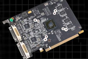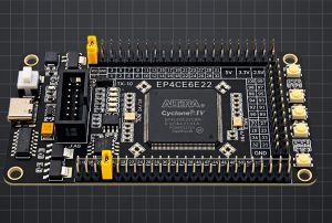

The design of modern robots has long transcended the mere assembly of mechanical structures, evolving into a precision engineering discipline that highly integrates mechanics, algorithms, perception, and power electronics.
Within the overall robotic hardware architecture, printed circuit board (PCB) assembly and circuit design/layout serve as the robot’s “nervous system” and “circulatory system.”
For diverse robot types—such as mobile robots, collaborative robotic arms, and humanoid robots—circuit design must not only meet constraints for miniaturization and lightweight construction but also maintain extreme reliability amidst strong electromagnetic interference, intense mechanical vibration, and complex, fluctuating load conditions.
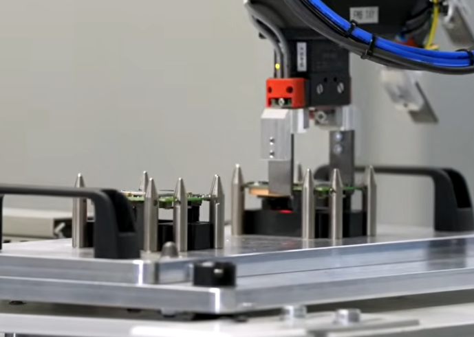
Traditional, rudimentary design approaches—such as proceeding directly to auto-routing after completing the schematic—are no longer adequate for the demanding environments of modern robots, where high-speed digital signals, high-power motor drives, and low-level sensor signal acquisition coexist.
This article provides an in-depth analysis of the professional nuances of robot PCB circuit design and layout, covering key aspects such as core architectural planning, power and drive systems, core processing units, sensor interfaces, thermal management and mechanical integration, and the application of modern design tools.
I. Core Challenges and Architectural Planning in Robot PCB Design
The Multidimensional Complexity of Robotic Electronic Systems
Electronic systems within robots exhibit a high degree of heterogeneity. Compact PCBs often simultaneously host high-voltage, high-current power circuits (ranging from tens to hundreds of volts), high-amperage switching power supplies, low-voltage digital logic circuits (operating at a few volts), and sensitive analog sensor signals at the microvolt or millivolt level.
This coexistence of high- and low-power circuits, along with the intertwining of high-speed signals and high-power operations, presents significant electromagnetic compatibility (EMC) challenges. From the outset, the system’s electrical architecture requires comprehensive planning to define signal flow and energy boundaries; this prevents high-frequency noise from causing false triggering in sensitive control units or sudden high-power current surges from triggering system resets.
Spatial Isolation Principles for Power, Control, and Sensing Layers
In robotic circuit layout, “zonal isolation” is a fundamental rule for ensuring stable system operation. Spatial layout must strictly adhere to the principle of functional partitioning, dividing the PCB into distinct zones: power drive, core processing, analog sensing, and communication interface.
(1) The power drive zone is typically positioned near the edges—close to power inputs and motor interfaces—to shorten high-current traces and minimize parasitic inductance and radiated interference.
(2) The core processing zone (housing components such as MCUs, DSPs, FPGAs, and SoCs) should be located in the center of the board or away from high-power heat sources to ensure the stability of logic operations.
(3) The analog sensing zone (containing components like IMUs, force sensors, and encoder conditioning circuits) must be kept away from sources of electromagnetic radiation. It requires protection via an independent local reference plane to prevent motor commutation noise from coupling into sensitive measurement circuits through the ground plane.
High-Level Trade-offs: Reliability, Thermal Management, and Interference Immunity
Robots often operate in harsh physical environments, enduring frequent start-stop shocks, mechanical vibrations, and temperature fluctuations.
Consequently, multi-objective trade-offs must be addressed during the architectural planning phase: high-power components require placement near PCB edges or the inclusion of dedicated copper heat-dissipation blocks for thermal management; heavy components and connectors need additional mechanical mounting points or adhesive reinforcement to withstand vibration; and high-speed signal traces must avoid board edges and areas of structural stress concentration to maintain signal integrity.
System-level planning at this high level allows for the deep integration of electrical performance with physical durability.
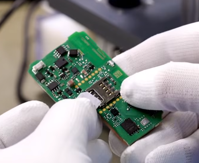
II. The Art of Layout: Power Supply and Drive Circuits
High-Current Paths and Parasitic Inductance Suppression
Robot joint actuation and chassis mobility rely on high-power motors, resulting in extremely high rates of change for transient currents (di/dt) within the drive circuits. According to the law of electromagnetic induction, even minute stray inductance can generate massive induced electromotive force (voltage spikes) during high-speed switching; this can not only cause dielectric breakdown in power MOSFETs or IGBTs but also radiate intense electromagnetic interference.
- (1) Power circuit traces must adhere to the “short, wide, and straight” principle; large copper pours should be used instead of thin traces whenever possible, and routing must remain symmetrical to balance the impedance of each branch.
- (2) Input filter capacitors (especially high-frequency ceramic capacitors and low-ESR electrolytic capacitors) must be placed immediately adjacent to the driver chip’s power pins to minimize the loop area for high-frequency pulsed currents, thereby reducing parasitic inductance to a minimum.
Thermal Design for H-Bridge and Motor Driver Chips
Modern robots commonly utilize brushless DC (BLDC) motors or stepper motors; their H-bridge drive circuits or Intelligent Power Modules (IPMs) are the primary sources of heat generation.
- (1) During layout, the PCB’s copper foil should be effectively utilized as a heat dissipation surface; a dense array of thermal vias should be designed beneath power components to rapidly conduct heat to internal PCB layers or to large copper heat-spreading areas on the bottom layer.
- (2) For power components that generate significant heat, space must be reserved for mounting metal heat sinks or thermal pads. Additionally, adequate thermal clearance must be maintained between these components and surrounding control circuits or sensitive elements to prevent parameter drift or thermal shutdown caused by localized overheating.
Noise Isolation: Single-Point vs. Multi-Point Grounding for Digital, Analog, and Power Grounds
Grounding is the most critical yet error-prone aspect of power supply layout. Robotic systems typically involve multiple ground planes: power ground (PGND), digital ground (DGND), and analog ground (AGND).
- (1) Blindly adopting a “unified” single ground plane is strictly prohibited, as is relying on crude “single-point isolation via thin traces.”
- (2) In practical layout, the power ground carries high currents and should utilize a dedicated, thick copper layer (e.g., 2oz or 3oz heavy copper); the digital ground provides a reference for logic switching; and the analog ground provides a noise-free reference for low-level signals.
- (3) Ultimately, all ground planes should converge at a single point—such as the power input or a specific low-impedance physical location on the system—using a “Star Grounding” topology, or be isolated at high frequencies via ferrite beads or 0-ohm resistors. This ensures that return paths for high-current loops do not flow through sensitive analog front-end circuitry.

III. Key Routing Principles for Microcontrollers and Core Processing Units
Impedance Matching and Crosstalk Control for High-Speed Signals
As the computational power of robots increases dramatically, data transmission rates between the main control chip and peripherals have reached the 100 Mbps or even Gbps range (e.g., Ethernet, CAN FD, MIPI camera interfaces, SPI buses, etc.).
- (1) For these high-speed signals, the characteristic impedance of transmission lines (e.g., 50 ohms for single-ended, 100 ohms for differential) must be strictly controlled; dielectric thickness and trace width should be calculated during the PCB stack-up design phase.
- (2) Differential traces must maintain strict length matching and tight coupling, and must not cross split planes, in order to preserve the common-mode rejection ratio (CMRR).
- (3) Adjacent signal layers should utilize “orthogonal routing”—routing horizontally on one layer and vertically on the next—to minimize capacitive crosstalk caused by parallel coupling between traces.
Precision Network Configuration of Decoupling Capacitors
When microcontrollers (MCUs), digital signal processors (DSPs), and FPGAs perform high-speed operations, the frequent switching of internal transistors causes significant fluctuations in instantaneous current, leading to momentary drops in supply voltage (power supply noise).
- (1) A precise network of decoupling capacitors must be configured for every power supply pin.
- (2) Capacitor values should be selected in a graded arrangement (e.g., 10μF, 1.0μF, 0.1μF, 0.01μF). High-frequency decoupling capacitors with low capacitance values must be connected to the chip’s power and corresponding ground pins via the shortest possible path (adhering to the “close proximity” principle); vias should be placed directly next to the pads, and long connecting leads are strictly prohibited.
Fan-out Strategy for BGA Packaging Areas
High-density robot motherboards frequently utilize BGA (Ball Grid Array) chips with high pin counts. Designing the fan-out for such a dense array of pads serves as a true test of a PCB engineer’s expertise.
- (1) Strategically plan the use of blind and buried vias, leveraging micro-via technology to free up routing channels on internal layers.
- (2) Carefully weigh the choice between “thermal relief” (cross-hatched) connections and “direct connections” (solid connections) for power and ground pads: use direct connections for power/ground pads carrying high currents to minimize impedance, while using thermal relief connections for standard signal pins to ensure solderability.
IV. Layout of Sensor Interfaces and Low-Level Signal Conditioning Circuits
Magnetic Interference Protection for Microvolt-Level Analog Signal Acquisition
Tactile sensors, high-precision load cells, and current-sensing resistors in robots often output weak analog signals in the microvolt or millivolt range; these are highly susceptible to interference from ambient power-frequency electromagnetic fields and switching noise from motor drives/inverters.
- (1) Analog signal traces must be kept as short as possible and protected using differential pair routing (twisted pair style) or thickened, shielded guard traces.
- (2) Critical components—such as operational amplifiers, ADCs, and their associated precision resistors and capacitors—should be placed in “clean zones” away from transformers, inductors, and high-power traces. Where necessary, design landing pads on the PCB for local metal shielding cans.
Routing Specifications for Differential Signals and Long-Distance Buses (CAN/RS485)
Long-distance communication between robot joint modules, or between the main controller and limb units, typically relies on CAN or RS485 buses.
- (1) Bus traces must be routed with strict parallelism and consistent spacing, and kept well away from motor drive circuitry and high-voltage switching power supplies.
- (2) Termination resistors (e.g., 120-ohm resistors) must be precisely placed at both ends of the physical transmission line, immediately adjacent to the transceiver chips, to eliminate signal reflections.
- (3) A robust protection network comprising TVS diodes, varistors, and common-mode chokes must be incorporated at the interface to prevent electrostatic discharge (ESD) and electrical fast transient (EFT) bursts—common in industrial environments—from damaging the communication interface.
RF Traces and Keep-out Zones for RF and Wireless Communication Modules
Modern mobile robots (such as AGVs, AMRs, and quadruped robots) commonly integrate Wi-Fi, Bluetooth, UWB (Ultra-Wideband) positioning, or 5G communication modules.
- (1) The layout of wireless RF circuits requires extreme precision; RF traces must maintain a characteristic impedance of 50 ohms. Right-angle or acute-angle bends are strictly prohibited; traces must utilize rounded corners or 45-degree angles.
- (2) A strict “Keep-out Zone” must be defined around the RF antenna. All metal layers, copper pours, and traces within this area must be cleared away to prevent surrounding dielectric materials and ground planes from absorbing the antenna’s radiated energy, thereby ensuring the robot’s wireless communication range and stability.
V. Co-design of PCB Thermal Management and Mechanical Structure
3D stacking and board-to-board interconnection within confined robotic spaces
Given the premium on internal space within robots, PCBs often cannot be laid out horizontally; instead, techniques such as multi-layer 3D stacking, vertical daughterboards, or Rigid-Flex PCBs are employed.
- (1) PCB stack-up design should adhere to the “symmetry principle”—sandwiching signal layers between solid ground or power planes—to prevent board warping or deformation during the reflow soldering process.
- (2) The layout of board-to-board connectors (such as high-density, high-speed connectors) must account for mechanical assembly tolerances, ensure contact reliability after repeated mating cycles, and avoid placing brittle surface-mount components in areas subject to bending stress.
Copper foil thickness, via-based heat dissipation, and thermally conductive fillers: For high-power robotic control boards, standard 1 oz (35 μm) copper thickness is often insufficient to carry currents of tens of amperes; consequently, heavy copper boards (2 oz, 3 oz, or thicker) or copper inlay processes must be utilized.
- (1) In areas with concentrated heat generation, in addition to increasing surface copper thickness, a high-density array of thermal vias should be strategically distributed to conduct heat to the heat-dissipating baseplate at the bottom.
- (2) Highly thermally conductive, electrically insulating silicone pads (thermal pads) should be placed between the PCB and the structural aluminum alloy housing to facilitate efficient, fanless passive cooling.
Structural reinforcement and stress relief in vibration and shock environments: Robots generate continuous high- and low-frequency mechanical vibrations during operation. Improper PCB layout can turn solder joints into stress concentration zones, making them highly susceptible to fatigue failure.
- (1) Heavy components (such as large electrolytic capacitors, transformers, and bulky connectors) must not be secured solely by surface-mount pads; mechanical retention clips, screw mounts, or epoxy adhesive reinforcement (dotting) must be incorporated into the design.
- (2) Mounting screws should be evenly distributed along the edges and corners of the PCB to prevent violent resonance at the board’s center caused by the cantilever effect during vibration.
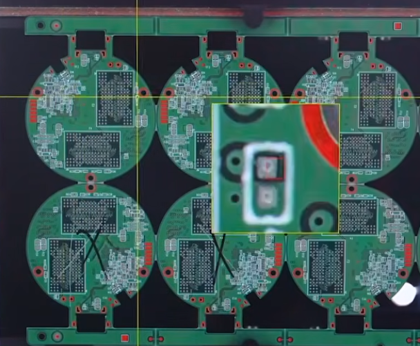
VI. The Future Landscape of AIGC-Empowered PCB Design for Modern Robots
AI-Assisted Optimization of Automated Layout and Routing
As the complexity of robotic circuitry grows exponentially, traditional manual layout and routing methods are reaching the limits of efficiency and performance.
- (1) Leveraging AIGC algorithms, modern intelligent design tools can automatically generate thousands of candidate layout schemes based on netlist connectivity from schematics, heat source distribution weights, and electromagnetic compatibility (EMC) constraints.
- (2) AI engines can automatically identify high-speed signal flow paths and optimize topologies, significantly shortening critical signal trace lengths and minimizing the adverse impact of parasitic parameters on system performance.
Intelligent Thermal Simulation and Signal Integrity Prediction
- (1) Prior to physical PCB fabrication, AI-integrated simulation software can complete full-board 3D thermal-fluid and electromagnetic (EMC/EMI) full-wave simulations within minutes.
- (2) Designers can visualize PCB surface temperature maps and current density distributions, promptly identifying potential thermal hotspots and crosstalk risks. They can perform one-click iterative optimizations in a virtual environment, marking a fundamental shift from “post-facto remediation” to “pre-emptive perfection.”
Design for Manufacturability (DFM) Checks and Failure Prediction
- (1) Modern AIGC-driven DFM tools can intelligently detect subtle flaws often overlooked in manual designs, such as insufficient pad spacing, improper stencil aperture designs, risks of the “tombstoning” effect, and potential panelization stress issues.
- (2) By incorporating big-data analysis of historical failure cases, AIGC can also predict the reliability and lifespan of robotic PCBs in extreme environments, ensuring that robotic hardware achieves aerospace-grade ruggedness and reliability before leaving the factory.
Summary
Robot PCB assembly and circuit design layout constitute a sophisticated systems engineering discipline that integrates power electronics, signal integrity, electromagnetic compatibility, thermodynamics, and mechanical engineering.
As an industry-leading hardware solutions provider, KingTop Technology transcends the limitations of single-discipline thinking; we begin with top-level architectural planning and exercise rigorous control over every detail—from high-current paths and high-speed signal impedance to precision analog isolation and thermal management.
By actively embracing the revolution in intelligent design tools driven by AIGC and deeply integrating advanced manufacturing processes with stringent standards, we create “electronic hearts” for modern intelligent robots—delivering rock-solid stability and superior performance even under extreme operating conditions for our global clients.