At the forefront of modern intelligent manufacturing, industrial robots are evolving from traditional systems—characterized by fixed-trajectory, heavy-load operations using mechanical arms—into industrial AI robots driven by Embodied AI, visual and force-control sensing, multi-axis coordination, and edge computing capabilities.
This shift in the technological paradigm presents rigorous challenges and entirely new requirements for the Printed Circuit Board Assembly (PCBA) factories that produce the “brains,” “nerves,” and “hearts” of these robots.
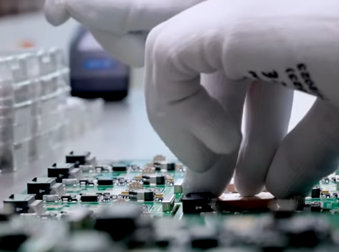
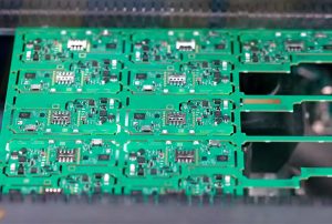
Unlike standard consumer electronics or general industrial PLC motherboards, the PCB and PCBA designs for industrial AI robots feature a complex combination of characteristics: ultra-high-density interconnects (HDI); high-frequency, high-bandwidth AI edge computing (generating significant heat); high-power motor servo drives (handling high currents); and microsecond-level, real-time multi-axis bus responses (requiring high interference immunity).
Drawing on frontline engineering experience in high-reliability PCB layout, fabrication, and Surface Mount Technology (SMT) assembly, this article provides an in-depth analysis of the technical complexities, core manufacturing processes, and quality control systems involved in industrial AI robot PCBA, as well as the practical implementation of AI manufacturing technologies in modern PCBA facilities.
I. Technical Characteristics and Unique Challenges of Industrial AI Robot Circuit Boards (PCB/PCBA)
The system architecture of an industrial AI robot comprises four core modules: the edge AI computing motherboard (the brain), multi-axis servo drive boards (the muscles), high-precision sensor array boards (the sensory/nervous system), and safety and power management systems (the heart).
This high level of system integration presents factories with extremely complex physical and electrical challenges during the production of these PCBs and PCBAs:
Edge AI Computing Motherboards: Balancing High-Density Interconnects and Thermal Management
Industrial AI robots must execute complex models—such as computer vision, SLAM (Simultaneous Localization and Mapping), and robotic arm path planning—locally and in real-time. These systems typically utilize components such as the Nvidia Jetson AGX Orin, industrial-grade SoCs from Qualcomm or Rockchip, or proprietary NPUs.
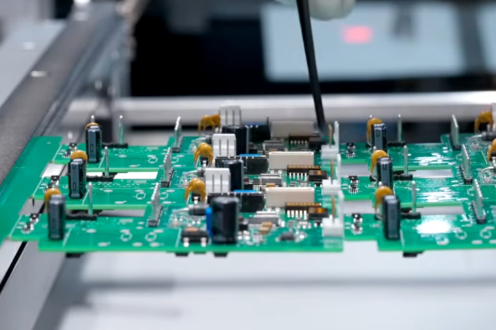
High Layer Count and Micro-via Technology (HDI): The chips utilize high-density BGA packaging (typically with pitches of 0.4mm–0.6mm and pin counts in the thousands). The PCB requires a third-order or even “Any-layer” HDI structure, employing laser micro-vias (blind/buried) and Via-in-Pad technology combined with resin filling and planarization (POFP).
High-Frequency Signal Integrity (SI): The board integrates PCIe 4.0/5.0, GMSL/MIPI image interfaces, and Gigabit/10-Gigabit Ethernet. Characteristic impedance must be strictly controlled (typically 85Ω/100Ω differential, 50Ω single-ended), and low-loss materials (Low Dk/Df)—such as Panasonic Megtron 6 or Rogers high-frequency composites—must be selected.
Extreme Heat Generation and Thermal Design: The core AI module consumes between 30W and 100W of power. During the layout and fabrication stages, designs incorporating large-area metal substrates or thick copper layers, copper inlays, or thermal via arrays are required to ensure rapid heat transfer to the robot’s integrated housing.
Servo Drive and Power Mainboard: High-Current Handling and High-Voltage Isolation
Industrial robot joints are driven by brushless DC (BLDC) or AC servo motors, with instantaneous peak currents reaching tens or even hundreds of amperes.
Heavy Copper Technology: Power and drive layers typically utilize 3oz to 6oz (or even 10oz) copper foil to handle high currents while minimizing line losses and temperature rise.
High-Voltage/Low-Voltage Electrical Isolation and Creepage Distance: Strict adherence to safety standards such as IEC 61800-5-1 is required between the high-voltage drive zone and the low-power control signal zone. Adequate creepage distances and electrical clearances must be maintained, and arc-prevention isolation slots must be incorporated into the PCB design.
Multi-axis High Interference Immunity (EMC/EMI) and High Reliability
Industrial environments are rife with strong electromagnetic interference (from sources such as variable frequency drives, arc welders, and high-power inductors). Motherboards for industrial AI robots must meet extremely rigorous industrial-grade interference immunity standards (IEC 61000-4 series):
Multilayer Board Stack-up Optimization: A strictly symmetrical “Signal Layer – Ground Layer – Power Layer – Ground Layer” structure is employed to create an effective Faraday cage shielding effect.
Resistance to Mechanical Stress and Thermal Shock: Continuous vibration occurs during robot movement and high-speed picking operations; therefore, the PCBA manufacturer must ensure high fatigue strength for solder joints. Substrate materials must feature a high glass transition temperature (High Tg ≥ 170 °C), high decomposition temperature (Td), and a low Z-axis coefficient of thermal expansion (CTE).
II. Analysis of the Complete PCBA Assembly and Manufacturing Process for Industrial AI Robots
Transforming a bare PCB into a highly reliable finished PCBA involves a series of rigorous, precision manufacturing steps subject to multiple quality checkpoints.
DFM (Design for Manufacturability) and Pre-production Review
Before the design enters the SMT production line, the Product Engineering (PE) team conducts an in-depth DFM/DFA review of the customer’s PCB Gerber files and Bill of Materials (BOM) using professional software such as CAM350 and Valor DFM:
Verify the ratio between stencil apertures and pads for 0.4mm pitch BGAs to prevent bridging or cold solder joints.
Evaluate the spacing between high-heat-generating components and heat-sensitive components. Verify the thermal relief pad design at the intersection of thick copper planes and standard signal traces to prevent cold solder joints caused by excessive heat dissipation during soldering.
High-Precision SMT (Surface Mount Technology) Assembly
High-Precision Solder Paste Printing (SPI Control): For 0201/01005 micro-components and 0.4mm pitch BGAs, fully automatic high-precision printers equipped with nano-coated electroformed stencils are utilized. Post-printing, 100% inspection via 3D SPI (Solder Paste Inspection) is mandatory, focusing on solder paste volume, area, thickness, and offset to eliminate over 80% of soldering defects at the source.
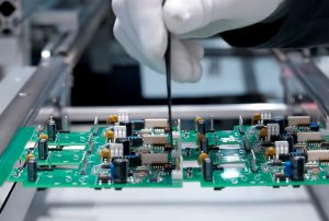
High-Speed, High-Precision Pick and Place: State-of-the-art pick-and-place machines (e.g., modular mounters) featuring AI-based visual alignment are employed, achieving a placement accuracy of ± 0.025 mm. For chips equipped with 3D sensors, LiDAR, or AI cameras, modular nozzles and low-pressure placement controls are used to prevent damage to sensitive components.
Reflow Soldering with Nitrogen (N₂) Protection: A 10–12 zone, full-convection nitrogen reflow oven is used. The nitrogen environment reduces residual oxygen levels to below 300 ppm, significantly lowering the oxidation rate of high-heat components and thick copper substrates, improving wetting angle quality, and minimizing internal BGA voiding (maintaining a voiding rate < 10%).
DIP (Through-Hole Technology) and Selective Soldering
Motherboards for industrial AI robots often incorporate through-hole technology (THT) components such as high-current relays, industrial connectors, and large capacitors. Traditional full-board wave soldering poses a risk of thermal shock to previously mounted high-density SMT components.
Selective Wave Soldering Process: Employs a sequence of preheating, flux spraying, and localized selective jet soldering to precisely solder each THT (Through-Hole Technology) pin. This method avoids damaging surrounding high-density AI BGA chips and ensures a through-hole fill rate exceeding 75%–90%.
Critical Inspection and X-Ray Axial Tomography
3D AOI (Automated Optical Inspection): Inspects for visual defects such as incorrect components, reversed polarity, tombstoning, and bridging.
3D X-Ray (AXI – Automated X-Ray Inspection): Utilizes multi-angle slice scanning via X-rays for BGAs, QFNs, and bottom thermal pads to precisely calculate solder ball voiding rates and detect micro-bridging and internal cracks.
III. Specialized Reinforcement and Protection Processes for Industrial AI Robots
Industrial AI robots operate in harsh environments characterized by high vibration, high humidity, heavy dust, strong electromagnetic interference, and even high temperatures with oil contamination. Standard SMT soldering cannot guarantee the required 5–10 year design lifespan; therefore, deep reinforcement is essential.
Underfill Process
The BGA chips in industrial AI robots (such as AI SoCs, FPGAs, and DDR5/LPDDR5) are subjected to shear forces caused by the rapid starting and stopping of robot joints, making solder balls highly susceptible to micro-cracking.
Process: After BGA soldering and testing are complete, a single-component epoxy underfill adhesive is dispensed along the chip edges using a fully automated dispensing machine.
Function: The adhesive penetrates beneath the chip via capillary action to encapsulate the solder balls. Upon curing, it distributes mechanical stress across the entire chip surface, enhancing the BGA’s shock resistance and thermal cycling durability by a factor of 5 to 10.
Automated Conformal Coating
Robots frequently operate in environments exposed to moisture and metal dust (such as cutting and welding workshops).
Process Details: The factory utilizes fully automated multi-axis robotic coating machines to apply acrylic, polyurethane, or silicone-based conformal coatings. Selective spraying is performed on the PCB surface, carefully avoiding connectors, test points, and sensor optical windows.
Curing and Inspection: Following UV curing, a 100% inspection of coating thickness and coverage uniformity is conducted under UV lighting to ensure complete isolation against salt spray, moisture, and conductive dust.
Secondary Curing and Adhesive Reinforcement for Components (Red Glue/UV Glue)
Specialized red glue or UV structural adhesive is applied to reinforce larger components—such as SMD inductors, large capacitors, and tall connectors—ensuring the robotic units can withstand industrial-grade, high-severity drop and random vibration tests (e.g., IEC 60068-2-64).
IV. Implementation of Industrial AI Manufacturing Technology
“Using industrial AI technology to manufacture motherboards for industrial AI robots” represents a core competitive advantage for modern, high-end PCBA manufacturing facilities. While traditional PCBA manufacturing relies heavily on manual expertise, AI-enabled factories have transformed into data-driven, adaptive manufacturing environments:
Intelligent AOI (AI-AOI) Based on Computer Vision and Deep Learning
Traditional AOI relies on simple color thresholds and edge contrast, resulting in persistently high false alarm rates. This not only consumes significant manpower for manual verification (VRS) but also risks shipping defective products due to missed detections.
AI Algorithm Application: Implementation of Convolutional Neural Networks (CNN) and Transformer-based image recognition models, trained on datasets containing millions of defect samples (including cold solder joints, micro-bridging, solder encapsulation, and slight component misalignment).
Benefits: Reduces false alarm rates by over 80% and triples verification efficiency, while simultaneously enabling anomaly detection for previously unseen defects.
2. Predictive Maintenance and Equipment Digital Twins
SMT Equipment Condition Monitoring: AIoT sensors are deployed on pick-and-place nozzles, lead screws, reflow oven fans, and SPI/AOI optical lenses to collect real-time data on vibration, temperature, motor current, and light intensity attenuation.
Predictive Models: AI models analyze data fluctuations to predict nozzle wear and component rejection rate trends. They automatically alert engineers to replace spare parts before placement errors or equipment breakdowns occur, thereby minimizing unplanned downtime.
Machine Learning-Based Adaptive Optimization of Reflow Profiles (Smart Reflow Tuning)
Variations in copper foil distribution, board thickness, and component density across different PCB batches can lead to uneven heating during the reflow process.
AI Closed-Loop Control: By integrating thermodynamic simulations with neural network models, the system processes input data—such as the PCB’s physical Gerber structure and BOM distribution—to directly predict and output optimal temperature settings for each heating zone and the conveyor speed.
Real-Time Adjustment: Heating power is dynamically fine-tuned during production based on feedback from inlet board temperature sensors, minimizing solder joint voiding and thermal stress.
End-to-End Production Traceability System (MES + AI Vision Traceability)
Industrial AI robot motherboard manufacturing demands extremely high standards for quality traceability.
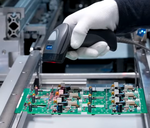
“One Board, One Code” (Laser Marking): A unique Data Matrix code is laser-etched onto each bare board upon entry into the factory.
End-to-End Intelligent Association: Image capture nodes for dispensing, placement, and soldering are installed along the entire SMT line. The AI system automatically links SPI solder paste data, placement offset data, real-time reflow temperature profiles, and X-ray cross-sectional images to the specific Data Matrix code. In the event of post-sales issues, the system enables rapid traceability—within seconds—to the specific raw material batch, production furnace run, or even the specific SMT nozzle ID.
V. Quality System and Testing/Validation for Industrial AI Robot PCBA Factories
High-reliability products are not merely manufactured; they are defined by rigorous testing and validation. Industrial AI robot PCBAs must pass multiple rigorous testing stages before leaving the factory:
+-------------------------------------------------------------------+
|               End-to-End Quality Verification System               |
+-------------------------------------------------------------------+
|
+--> 1. ICT (In-Circuit Test): Check for open/short circuits, resistance/capacitance values, and chip pin solderability
|
+--> 2. FCT (Functional Circuit Test): Simulate actual operating environments to perform full-function verification
|      +-- High-load operational test (AI module full load / compute power test)
|      +-- Industrial bus communication test (EtherCAT / CANopen packet loss rate)
|      +-- Multi-axis servo drive current response test
|
+--> 3. Industrial-Grade Burn-in Test
|      +-- High and low temperature cycling test (-40°C to +85°C)
|      +-- 85 High-Temperature & High-Humidity Aging Test (85°C / 85% RH)
|
+--> 4. Vibration & Shock Testing
1. ICT (In-Circuit Test): Uses a bed-of-nails fixture to test for open/short circuits, resistance, capacitance, and diode/transistor characteristics across various board networks, rapidly identifying basic SMT soldering defects.
2. FCT (Functional Test): Employs specialized intelligent test fixtures to simulate the robot’s actual operating environment:
- AI Computing Board Load Test: Runs inference stress test programs (e.g., TensorRT benchmarks) to drive the NPU/GPU to 100% utilization, while monitoring voltage ripple and temperature rise in onboard DC-DC power modules.
- Bus Communication Test: Measures packet loss rates and latency for EtherCAT, CANopen, RS485, and GMSL vision interfaces at maximum throughput (ensuring microsecond-level real-time response).
- Servo Drive Response Test: Connects a simulated load to test the response speed and over-current protection (OCP) sensitivity of high-voltage, high-current MOSFET/IGBT drive circuits.
3. Environmental Stress Screening (ESS / Burn-in Test): For industrial robot motherboards requiring high reliability,
high/low-temperature cycling (-40°C to +85°C) and high-temperature/high-humidity powered aging (85°C/85% RH) are performed—either via batch sampling or 100% inspection—to eliminate components prone to early-stage failure (infant mortality) before deployment.
VI. Future Outlook: Deep Integration of AI and Advanced Intelligent Manufacturing
With the explosive growth of the Embodied AI and Humanoid Robotics industries, the system complexity of industrial robots is increasing exponentially. Future circuit board assembly plants will continue to evolve in the following directions:
3D Assembly (3D MID & Embedded PCB): Directly printing or embedding circuits within the robot’s mechanical framework to achieve “board-less” structures and extreme space optimization.
Integration of higher-density Through-Silicon Vias (TSV) and advanced packaging: PCBA facilities are increasingly adopting semiconductor assembly and test (OSAT) processes to enable Chiplet and wafer-level System-in-Package (SiP) assembly.
Generative AI-empowered factory operations: Generative AI facilitates the creation of Design for Manufacturability (DFM) reports, automated production scheduling (APS), and intelligent troubleshooting assistants, further shortening the cycle from engineering drawings to sample delivery.
As a pioneer in high-end hardware manufacturing and the delivery of high-reliability circuit boards, KingTop Technology specializes in the R&D and PCBA manufacturing of industrial AI robots, AI edge computing nodes, and high-density servo drive motherboards. Leveraging a rigorous quality control system that adheres to IPC-A-610 Class 3 standards, deeply integrated AI-driven SMT assembly lines, and comprehensive hardware manufacturing and ruggedization services, KingTop Technology provides industrial robot clients with efficient, one-stop solutions—spanning PCB fabrication, SMT assembly, and protective ruggedization to full-function testing (FCT).
Serving as the physical bridge between software and hardware, modern PCB/PCBA manufacturing facilities—characterized by their industrial-grade reliability and intelligent AI-driven ruggedization and inspection technologies—are becoming the cornerstone for the global industrial AI robotics industry’s transition toward large-scale, high-quality mass production.