The booming robotics industry in China has driven rapid growth in the demand for high-end, high-density, and highly reliable PCB assemblies (PCBA).
Robotic electronic systems impose rigorous technical requirements on PCBA; they necessitate not only mixed-signal routing—handling both high-current power drive and low-level signal processing—but also the ability to withstand severe mechanical vibration, high-frequency thermal cycling, and complex electromagnetic interference (EMI).
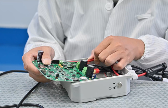
Catering to both industrial and consumer robotics applications, comprehensive one-stop PCB assembly solutions cover the entire process: from circuit design optimization, precision SMT placement, and high-reliability through-hole assembly (THT) to comprehensive testing and conformal coating.
I. Key Technical Aspects of Robotic PCB Assembly
High-Density Interconnect (HDI) and Multi-layer Board Technology
Blind/Buried Vias and Micro-via Technology: Utilization of 1st-order, 2nd-order, and Any-layer HDI technologies to effectively save motherboard space and meet the constraints of compact robotic joints and controllers.
Thick Copper and Thermal Design: For motor driver boards, thick copper processes (ranging from 2oz to over 6oz) are employed alongside Metal Core PCBs (MCPCB) or copper inlay technologies to enhance high-current carrying capacity and thermal dissipation efficiency.
Mixed-Signal and EMI/EMC Control
High/Low Voltage Isolation: Strict physical partitioning and ground isolation (via optocouplers or galvanic isolation) between high-voltage/high-current drive sections and low-level sensor sections on the same PCB.
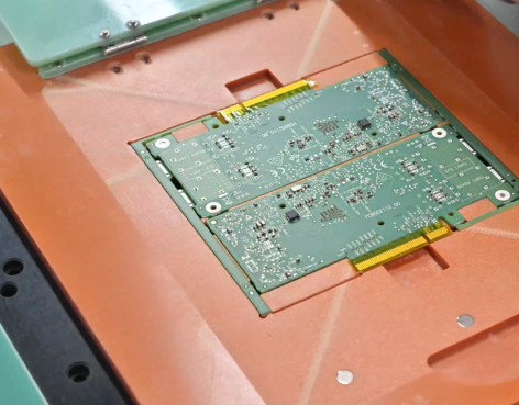
Signal Integrity: Precise impedance control and differential pair length matching for high-speed communication interfaces such as CAN bus, EtherCAT, USB 3.0, and LVDS.
High-Reliability Placement and Soldering Processes
Precision SMT Placement: Support for high-precision placement of miniature components (e.g., 01005, 0201) and fine-pitch chips (e.g., 0.3mm pitch BGA and QFN).
Selective Wave Soldering vs. Selective Soldering: Ensures sufficient solder joint fullness (fill rate >85%) for high-power pin-type interfaces and sensor sockets, preventing joint fractures in high-vibration environments.
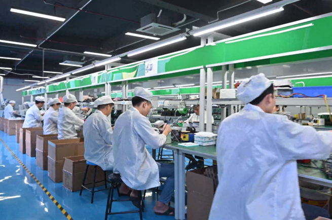
II. Robotic PCBA End-to-End Production and Process Specifications
Pre-SMT Preparation and DFM (Design for Manufacturability) Review
DFM/DFA Review: Conducts DFM/DFA checks on Gerber and BOM files prior to manufacturing, evaluating pad design, component spacing, stencil aperture ratios, and thermal balance.
Material Pre-treatment and Baking: Rigorous baking for chips and boards with high MSL (Moisture Sensitivity Level) ratings to prevent the “Popcorn Effect” during reflow soldering.
Surface Mount Technology (SMT) Line Control
Fully Automated Solder Paste Printing: Equipped with automatic stencil cleaning and SPI (Solder Paste Inspection) systems to monitor solder paste volume, area, and offset with 100% coverage.
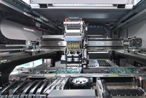
High-Speed, High-Precision Placement: Utilizes dual-track modular placement machines combined with vision alignment systems, achieving placement accuracy of ±0.025 mm.
Nitrogen (N₂) Reflow Soldering: Reflow soldering performed in a nitrogen-protected environment to reduce solder joint oxidation, improve wettability, and minimize voiding (Voiding Rate < 10%).
Quality Inspection and Post-Assembly
3D AOI and 3D X-Ray Inspection: Uses 3D X-Ray for non-destructive testing of BGA, QFN, and bottom-layer solder joints, accurately identifying cold joints, bridging, and voids.
Conformal Coating: Since robots often operate in dusty, humid, or oily environments, automatic selective coating machines apply acrylic, polyurethane, or silicone coatings to ensure protection against moisture, salt spray, and electrical leakage.
III. PCB Assembly Solutions for Core Robotic Modules
| Robot Core Module | Primary Process & Technical Features | Quality & Performance Assurance Focus |
| Main Control & Computing Board (AI/ROS Core) | Multi-layer HDI board, High-density BGA assembly, High-speed impedance control | Signal integrity testing, Via-fill planarity, High-temperature & high-humidity aging test |
| Servo/Stepper Motor Driver Board | Heavy copper PCB, High-current circuitry, Copper inlay / Thermal via array, Selective wave soldering | Overcurrent capability testing, Thermal imaging analysis, Solder joint fatigue resistance |
| Sensor Acquisition Board (LiDAR/IMU/Vision) | Miniaturized size, Rigid-Flex PCB, High-precision alignment | Sensor stress control, Anti-vibration underfill encapsulation |
| BMS Power Management Board | High-voltage isolation, High-power MOSFET assembly, Precision sampling resistor | Dielectric withstand voltage test, Thermal balance control, Safety protective coating |
IV. Quality System and Testing/Validation Standards
Industry Quality Standards: Production processes strictly adhere to IPC-A-610G Class 3 (the highest industrial/medical grade standard) and IATF 16949 quality management system certification.
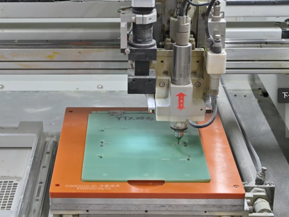
In-Circuit and Functional Testing (ICT/FCT):
ICT (Bed-of-Nails Testing): Detects open/short circuits, resistor and capacitor tolerances, and voltages at critical nodes.
FCT (Functional Testing): Involves firmware programming and the setup of simulation platforms to verify full functionality—including drive capability, communication response, and sensor data acquisition—under actual operating conditions.
Environmental and Reliability Testing:
Simulated transport vibration and random drop tests.
High/low-temperature cycling and thermal shock tests (-40°C to +125°C).
Full-load continuous power-on burn-in tests.
Summary
This Chinese robotic PCB assembly (PCBA) solution encompasses the entire design and manufacturing lifecycle. Its core strengths lie in strict adherence to the IPC-A-610G Class 3 standard and the use of HDI (blind/buried via) and thick-copper heat dissipation technologies to minimize size while handling high currents.
It ensures communication stability and interference resistance through high/low-voltage isolation and impedance control. Furthermore, the SMT process employs 01005 micro-component placement, nitrogen reflow soldering, 3D AOI/X-ray inspection, and automated conformal coating to meet stringent reliability requirements in high-density, high-vibration, and complex electromagnetic environments.