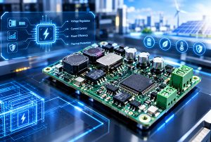
In high-power-density applications—such as power electronics, new energy vehicles, high-power industrial controls, and server power supplies—heavy copper power PCBs serve critical functions: conducting high currents, rapidly dissipating heat, and providing robust mechanical support.
Unlike standard signal-level PCB assembly, the manufacturing of heavy copper power PCB assemblies (PCBAs) involves challenges such as soldering with massive thermal capacity requirements, applying high-viscosity solder paste, mounting components subject to high mechanical stress, and executing rigorous insulation and protection processes.
The following is an in-depth technical analysis of the end-to-end manufacturing process for heavy copper power PCBAs.
I. Technical Characteristics and Manufacturing Challenges of Heavy Copper Power PCBs
Heavy copper power PCBs are generally defined as printed circuit boards with copper foil thicknesses exceeding 3 oz/ft² (approximately 105 μm), sometimes reaching 6 oz to 10 oz.
Their unique physical properties pose significant technical challenges for traditional SMT (Surface Mount Technology) and THT (Through-Hole Technology) assembly processes.
Massive Thermal Capacity and Heat Sink Effect: Heavy copper conductors (such as large-area power and ground planes) possess extremely high thermal conductivity and thermal capacity.
During reflow and wave soldering, heavy copper areas absorb heat rapidly, causing the solder pads to heat up slowly. Insufficient heat input can easily lead to defects such as false soldering, cold solder joints, and tombstoning. Conversely, indiscriminately raising the heating temperature may damage surrounding heat-sensitive components or cause substrate delamination.
Surface Topography and Solder Paste Printing Control: The etching depth for circuits on heavy copper boards is significant, resulting in a substantial step height difference (ranging from 70 to 150 μm) between the solder mask and the copper traces. This results in poor contact between the stencil and the board, making the process prone to squeegee leakage, solder paste slump at the edges, or bridging during printing.
Mechanical and electrical stresses on large, high-power components: Thick-copper motherboards often integrate bulky inductors, high-capacity electrolytic capacitors, MOSFET power modules, and high-current terminals.
Due to their significant weight and high lead rigidity, these components are prone to generating substantial mechanical and thermal stresses during placement, soldering, and thermal cycling, placing extremely high demands on the fatigue strength of the solder joints.
II. DFM (Design for Manufacturability) Optimization and Substrate Selection
The prerequisite for manufacturing highly reliable thick-copper PCBAs is the strict implementation of upfront DFM specifications.
Pad and Thermal Relief Design
Thermal pad and thermal via design: For through-hole leads located in large copper-pour areas, thermal relief pads must be used to prevent excessive heat dissipation during soldering caused by an overly large copper connection area.
Thermal via plugging process: It is recommended to use a resin-plugging and planar-plating process (VIPPO) for thermal vias located beneath power components; this prevents solder from flowing down the vias during reflow, which would otherwise result in insufficient solder on the pads.
Solder Mask and Stencil Aperture Matching
The solder mask covering the edges of thick-copper traces must be free of bubbles and peeling.
Stencil aperture design must account for the height difference (step) created by the thick copper; clearance designs or step stencils should be employed to ensure the precise deposition of solder paste onto high-density leads and power component pads.
III. Key Process Controls for SMT Assembly
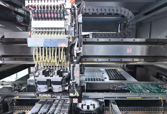
Stepped Stencil Design and High-Viscosity Solder Paste Application
Stepped Stencil (Step-up/Step-down): A “step-up” stencil design is employed in areas with thick copper and large-pin pads to increase solder paste deposition, while a “step-down” design is used in fine-pitch IC areas to prevent solder bridging.
Solder Paste Selection: Lead-free SAC305 or high-reliability silver-bearing alloy solder pastes with high metal content and high slump resistance are selected to ensure optimal wetting force and joint fullness in the molten state.
High-Power, Multi-Zone Reflow Soldering Profile Optimization: Reflow soldering for thick-copper motherboards requires a high-power nitrogen reflow oven with multiple zones (typically 10–12 zones). Key parameter controls are as follows:
Preheating Zone: The ramp-up rate is controlled at 1.0–1.5°C/s; a gradual temperature rise minimizes the temperature differential (ΔT) between the thick-copper substrate and large-mass components.
Soaking Zone: The soak time is extended to 90–120 seconds with the temperature maintained at 150–190°C, allowing the entire board (including large copper foil areas and small-signal areas) to reach thermal equilibrium.
Peak Zone: The peak temperature is set to 240–250°C, and the Time Above Liquidus (TAL) is extended to 60–90 seconds to ensure that high-thermal-mass pads absorb sufficient heat for adequate wetting.
Nitrogen Protection: Oxygen concentration within the oven is maintained below 500 ppm to prevent secondary oxidation of the thick copper at high temperatures and to improve the wetting angle of the solder joints.
IV. THT High-Current Components and Wave/Selective Soldering Processes
High-current components on power motherboards—such as transformers, inductors, and terminal blocks—typically utilize Through-Hole Technology (THT).
Selective Wave Soldering: For double-sided, mixed-technology power supply motherboards featuring thick copper, selective wave soldering is the preferred solution:
Independent preheating and soldering times can be applied to individual high-power through-hole components.
High-power electromagnetic pump nozzles are used to extend contact time, ensuring the molten solder rises to over 75% of the height within the thick-copper through-holes (compliant with IPC-A-610 Class 3 standards).
Press-Fit Technology: Solderless press-fit processes are increasingly adopted for ultra-high-current terminals (e.g., >100A). High-precision servo press-fit machines drive rigid pins into thick-copper metallized vias; mechanical connection and low-resistance electrical conduction are achieved through cold-weld deformation, completely eliminating defects associated with thermal soldering.
V. Thick-Copper PCBA Inspection, Cleaning, and Conformal Coating
Combined 3D AOI and 3D X-Ray Inspection
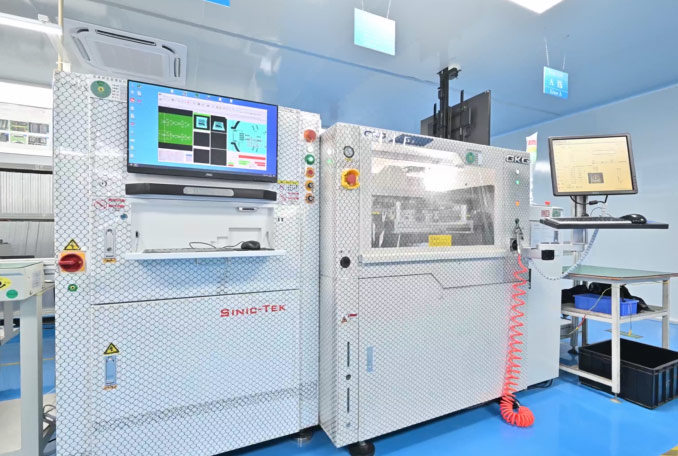
3D AOI: Used to detect issues such as tombstoning, misalignment, and solder wetting on large-volume components.
3D X-Ray (AXI): Solder pads for BGAs, QFNs, and power MOSFETs (e.g., D2PAK, DirectFET) located on the bottom of thick-copper boards are obscured by the copper; X-ray tomography is essential to inspect internal void rates. Void rates for pads under high-power devices must be strictly controlled (below 10%–15%) to prevent device burnout caused by increased thermal resistance.
Residue Cleaning: High-power power supply motherboards operate in high-voltage, high-current environments for extended periods; flux residues can easily trigger electrochemical migration (ECM) or current leakage. In-line aqueous cleaning systems combined with specialized water-based cleaning agents are required to thoroughly clean the PCBA, ensuring ionic contamination levels remain below 1.5 μg/NaCl eq./cm².
Conformal Coating: Power supply motherboards often operate in harsh industrial environments characterized by humidity, salt spray, and dust.
Automated selective coating machines are used to apply acrylic, polyurethane, or silicone conformal coatings.
To address issues such as exposed copper or thin coating films at the edges of thick-copper traces, coating viscosity is strictly controlled and secondary touch-up spraying is performed; this ensures that breakdown voltage and insulation resistance meet safety standards.
VI. Quality Control and High-Reliability Testing
To ensure the fault-free operation of thick-copper power supply motherboards throughout their lifecycle, the following testing procedures must be implemented:
100% ICT (In-Circuit Testing) and FCT (Functional Testing): Verifying the conduction resistance of high-current paths and output stability under rated loads.
Thermal Imaging Analysis: Using infrared thermal imagers during full-load FCT to monitor real-time temperature rises at various power nodes on the thick-copper motherboard, enabling the timely detection of hidden cold solder joints or high-resistance solder joints.
Thermal Cycling and Burn-in Testing: Conducting burn-in tests under load within a thermal cycling chamber (ranging from -40°C to +125°C) to induce and screen out products prone to early-life stress failures.
Conclusion
The assembly and manufacturing of thick-copper power supply motherboards is a systematic process that requires moving beyond the mindset of standard SMT processing.
From upfront DFM (Design for Manufacturability) regarding thermal resistance and stepped stencil fabrication, through high-energy reflow profile settings and selective wave soldering climb control, to 3D X-ray void inspection and high-insulation coating—every step must be precisely tailored to the core characteristics of “high thermal mass, high stress, and high current.” Only through this approach can high-quality, highly reliable core motherboards for power electronics be delivered.