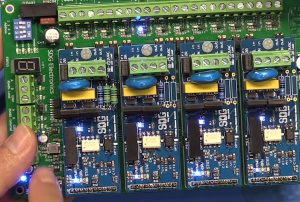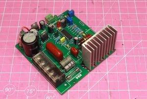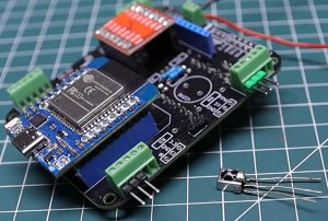

Driven by advancements in new energy, intelligent manufacturing, and high-end electronic equipment, traditional general-purpose power modules often fall short of meeting the specialized requirements for high power density, stringent electromagnetic compatibility (EMC), and specific circuit topologies.
As the core for power distribution and control within a hardware system, the design and manufacturing quality of a custom power control mainboard directly determine the overall performance and long-term reliability of the entire device.
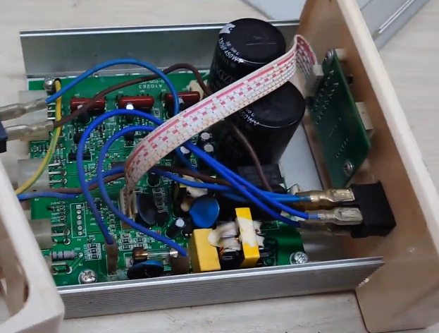
This article explores the core specifications and technical essentials of custom power control mainboard PCB assembly design—covering everything from system architecture planning, schematic design, and high-performance PCB layout to manufacturing processes (DFM for SMT and DIP assembly) and quality verification.
I. Custom Power Control Mainboard PCB Assembly Design
Definition and Functional Value of Custom Power Control Mainboards
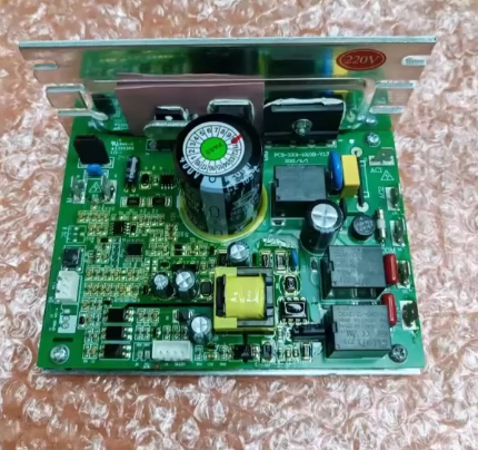
A custom power control mainboard is an integrated power management and control core developed specifically for particular application scenarios—such as industrial variable-frequency drives (VFDs), new energy inverters, smart charging piles, medical equipment, and high-end embedded systems.
Beyond facilitating efficient power conversion (e.g., AC-DC, DC-DC, or DC-AC), these boards integrate MCU/DSP-based digital signal processing, real-time voltage and current sampling, protection mechanisms, communication interfaces, and peripheral drivers.
Compared to standardized power modules, custom designs are precisely tailored to fit structural space constraints, meet specific electrical performance benchmarks, and accommodate multi-functional integration—thereby optimizing system costs and maximizing space utilization.
Requirements for High Reliability and Adaptation to Extreme Environments
In settings such as industrial sites, outdoor base stations, or automotive embedded environments, power control mainboards are frequently subjected to harsh conditions—including high temperatures, high humidity, intense electromagnetic interference (EMI), severe vibration, and significant fluctuations in grid voltage. Consequently, the design and assembly of custom power control mainboards must prioritize high reliability above all else.
This requires not only strict adherence to industrial or automotive-grade standards during component selection, but also the incorporation of redundancy—accounting for thermal, mechanical, and electrical stresses—throughout the PCB design phase to ensure fault-free operation over the system’s entire lifecycle.
The Role of Intelligence and AIGC in Power Supply Design
With the proliferation of artificial intelligence, AIGC tools and automated design scripts are playing an increasingly vital role in the R&D process for power control boards. From schematic logic verification and PCB routing optimization to thermal simulation analysis, these intelligent tools significantly shorten development cycles and reduce the incidence of human design errors.
Furthermore, control boards equipped with digital power management (PMBus/SMBus) capabilities enable real-time status monitoring, self-diagnostics, and adaptive parameter adjustment—laying a robust foundation for the development of intelligent, digitized, and eco-friendly energy systems.
II. Circuit Architecture and Schematic Design Essentials for Power Control Boards
Selection of the Main MCU/DSP and Peripheral Circuit Planning
The “brain” of a power control board is typically a high-performance microcontroller (MCU) or digital signal processor (DSP). During the schematic design phase, the chip must be selected based on the complexity of the control algorithms (such as advanced PID control or SVPWM modulation). Key evaluation criteria include clock frequency, the number of PWM output channels, ADC sampling precision, and available communication interfaces (e.g., CAN, RS485, SPI, or I2C).
Power Decoupling Design: High-frequency decoupling capacitors—typically a combination of a 0.1µF ceramic capacitor in parallel with a 10µF electrolytic or tantalum capacitor—must be placed near the power pins of each chip to filter out high-frequency noise and ensure a highly stable power supply for the core processor.
Reset and Clock Circuits: The crystal oscillator circuit should be positioned as close to the MCU as possible, using short, wide traces surrounded by a ground plane (ground shielding) to prevent external electromagnetic interference from causing system freezes or erratic program execution.
Power Conversion Topology Design and Component Matching
Selecting an appropriate switching power supply topology—based on input/output voltage, power rating, and efficiency requirements—is the core task in schematic design.
Topology Selection Comparison Table:
| Application Scenario | Recommended Topology | Power Range | Core Advantages |
| Low-power auxiliary power supply | Flyback | 5W – 100W | Simple circuit, low cost, easy multi-output support |
| Medium-power industrial power supply | Forward / Half-Bridge | 100W – 500W | High transformer utilization, low output ripple |
| High-power & new energy | Phase-Shift Full-Bridge / LLC Resonant | 500W – Several Kilowatts | High efficiency, good soft-switching characteristics, low electromagnetic interference |
Power Device Selection: When selecting MOSFETs or IGBTs, ensure sufficient voltage and current margins (typically by derating voltage stress to below 70% and current stress to below 50%). Rigorously calculate conduction and switching losses to provide accurate data for subsequent thermal design.
Isolation and Protection Circuit Design
Power control boards often involve the interaction between high-voltage/high-power circuits and low-voltage/low-power control circuits. Electrical isolation is critical for ensuring personnel safety and protecting equipment from surge transients.
Signal Isolation: Use optocouplers (e.g., TLP series) or digital isolators (e.g., ISO series) to provide robust isolation for PWM drive signals and feedback sampling signals.
Protection Mechanisms: The schematic must incorporate comprehensive protection circuits, including Over-Voltage Protection (OVP), Over-Current Protection (OCP), Over-Temperature Protection (OTP), and Short-Circuit Protection (SCP). For shunt resistors, employ a Kelvin four-terminal connection method to eliminate sampling errors caused by lead resistance.
III. High-Performance PCB Layout and Routing Engineering Standards
High/Low-Voltage Isolation and Safety Spacing (Creepage & Clearance)
A core safety principle in the design of power control PCBs is ensuring that the clearance and creepage distances between the high-voltage side and the low-voltage side comply with relevant national and international standards (such as IEC 60950 or IEC 62368).
Physical Slots (Cutouts): Implement physical isolation slots (cutouts) between the high-voltage and low-voltage regions of the PCB. Ensure that no copper traces or solder mask exist within these slots to effectively prevent high-voltage arcing or breakdown.
Components Spanning the Isolation Barrier: Do not route any traces beneath components that bridge the isolation barrier—such as transformers, optocouplers, or safety-rated capacitors. If necessary, remove the copper (create a cutout) in the underlying layers.
High-Current Trace Routing and Thermal Design
Power control boards contain multiple high-current paths (such as input rectification circuits, paths from power switching transistors to transformers, and output rectification and filtering circuits).
Optimization of Copper Thickness and Trace Width: It is recommended to use copper foil with a thickness of 2 oz (ounces) or greater to reduce DC resistance and temperature rise in high-current traces. Trace widths should be precisely calculated based on the IPC-2152 standard to ensure they can accommodate the required current.
Power Plane Partitioning in Multilayer Boards: For multilayer board structures, it is advisable to use dedicated internal power planes to carry high currents, thereby avoiding voltage drops associated with long, narrow traces. Additionally, an array of thermal vias should be strategically placed to efficiently conduct heat generated by power components to a large copper area on the opposite side of the board or to an external heatsink.
EMI/EMC-Resistant Routing and Ground Plane Partitioning
Electromagnetic Compatibility (EMC) is a key metric for evaluating the quality of a power control board.
Grounding Strategy: System grounds should be partitioned into Power Ground (PGND), Digital Ground (DGND), and Analog Ground (AGND), and connected at a single point (Star Grounding). This prevents high-current switching noise from coupling into sensitive analog sampling circuits.
Protection of Sensitive Signals: The copper area of switching nodes (SW nodes) should be kept as small as possible to minimize parasitic capacitance and high-frequency radiation. High-frequency control signal traces (such as those for crystal oscillators, reset signals, or PWM signals) should be routed away from strong magnetic field sources like transformers and inductors; where necessary, guard rings (ground traces surrounding the signal) should be employed for shielding.
IV. SMT (Surface Mount Technology) and DIP (Through-Hole) Process Design (DFM)
Design for Manufacturing (DFM) Specifications and Stencil Aperture Optimization
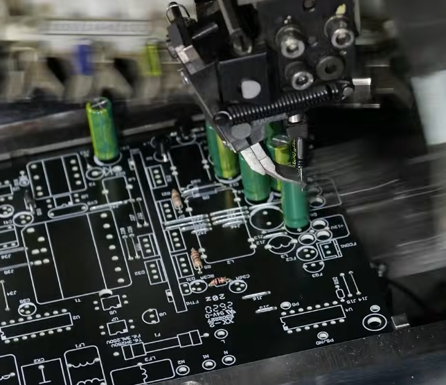
Before proceeding to the PCB manufacturing and assembly stages, a rigorous DFM (Design for Manufacturing) review must be conducted to ensure that the design aligns with the process windows required for high-speed SMT placement and soldering.
Pad Design: Pads for surface-mount components (such as those in 0603 or 0805 packages) and IC pins should be designed symmetrically to prevent the “tombstoning” defect caused by uneven heating during the reflow soldering process.
Stencil Aperture: For large-area pads on power components (e.g., the thermal pads at the bottom of TO-220 or DPAK packages), the stencil apertures should be designed in a “window pane” (grid) or cross-pattern. This limits the solder paste release to between 50% and 70%, effectively preventing excessive voiding—which could otherwise lead to overheating and component burnout.
Component Selection and Bill of Materials (BOM) Management
The BOM for a power control motherboard often includes a variety of specialized components, such as high-voltage electrolytic capacitors, magnetic components (transformers, common-mode inductors), high-power ceramic capacitors, and precision metal-film resistors.
Package Consistency: Ensure that the package codes for all components in the BOM strictly match those in the PCB library files.
Temperature and Voltage Ratings: For all components—especially capacitors, ferrite beads, and semiconductor devices—the temperature ratings (e.g., 105°C or 125°C for electrolytic capacitors) and voltage ratings must include an engineering margin of 15% to 20%.
Process Parameter Setting and Defect Prevention for Reflow and Wave Soldering
SMT Reflow Soldering Temperature Profile: Carefully configure the temperature profiles for the preheat, soak (thermal equilibrium), reflow, and cooling zones.
When using lead-free solder (such as SAC305), the peak temperature should be maintained between 240°C and 250°C. The duration in the reflow zone must be well-balanced to ensure bright, well-wetted solder joints.
DIP (Through-Hole) Assembly and Wave/Selective Wave Soldering: For large components that cannot be mounted via SMT—such as large transformers, connectors, and heatsinks—a DIP (through-hole) assembly process must be used. Power supply boards often feature large copper-foil heat-dissipation areas, which can lead to “cold” (incomplete) solder joints or solder bridging during wave soldering. To ensure that through-hole solder joints are robust and reliable, the use of selective soldering or localized preheating via specialized fixtures is recommended.
V. Quality Control, Verification, and Reliability Testing (DVT/PVT)
Automated Optical Inspection (AOI) and X-Ray Non-Destructive Testing
AOI: High-speed AOI is performed immediately after SMT reflow soldering to comprehensively detect surface defects such as missing components, incorrect parts, misalignments, reversed orientation, and solder bridging.
X-Ray Inspection: For components like QFN-packaged chips with bottom thermal pads, power MOSFETs, and high-power modules, industrial-grade X-Ray equipment must be used for non-destructive testing. This ensures strict control over the void ratio within the solder pads (typically requiring the void area to be less than 20%–25% of the total pad area) to prevent thermal breakdown caused by increased thermal resistance from voids.
In-Circuit Testing (ICT) and Functional Circuit Testing (FCT) Fixture Design
ICT: A “bed-of-nails” tester is used to precisely check for open circuits, short circuits, and the static electrical parameters of components (such as resistance, capacitance, and diode voltage drops) on the PCB.
FCT: Custom-designed FCT test benches are employed to conduct fully automated, comprehensive testing. By simulating actual operating loads and input voltage ranges, the system verifies the output voltage accuracy, ripple factor, dynamic response time, protection thresholds, and communication functions of the power control board, ensuring zero defects in the final product.
Burn-in Testing, Environmental (High/Low Temperature) Testing, and EMC Pre-certification
Burn-in Test: Assembled power control boards are placed in a high-temperature burn-in chamber and operated under rated full-load conditions for at least 48 consecutive hours to screen out components prone to early-life failure.
Environmental and EMC Testing: Based on the product’s final application standards, testing—including high/low-temperature cycling, vibration, and EMC pre-certification (such as Electrostatic Discharge (ESD), Surge, Conducted Emissions (CE), and Radiated Emissions (RE))—is conducted to ensure the motherboard operates stably and reliably within complex electromagnetic environments.
VI. Conclusion
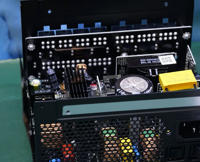
The design and PCB assembly of custom power control motherboards represent a systematic engineering endeavor that integrates power electronics, circuit design, high-speed PCB layout, Design for Manufacturing (DFM), and quality control.
The optimization of every design detail directly influences the product’s final conversion efficiency, thermal management, and long-term reliability. With the widespread adoption of third-generation semiconductor materials—such as Silicon Carbide (SiC) and Gallium Nitride (GaN)—power control motherboards are rapidly evolving toward higher switching frequencies, greater power density, and full digitalization.
Future power PCB design requires engineers not only to possess a solid foundation in traditional analog and digital circuits but also to stay at the forefront of developments in intelligent manufacturing and AIGC-assisted design. By continuously pushing technical boundaries, engineers can deliver increasingly efficient, eco-friendly, and stable power control solutions for industries worldwide.