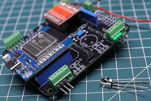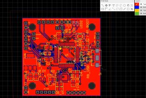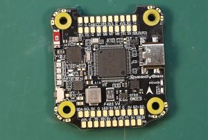

A motor controller serves as the critical hardware interface between a power source, control algorithms, and the motor itself. It is widely used in applications such as industrial automation, robotics, power tools, drones, home appliances, and new energy vehicles.
Typically, it integrates a main control MCU, gate drivers, power MOSFETs or IGBTs, current and voltage sensing circuits, protection circuitry, and communication interfaces.
A motor controller PCB does more than just interconnect components; it must maintain stability under demanding conditions, including high currents, rapid switching, temperature rises, mechanical vibration, and electromagnetic interference (EMI).
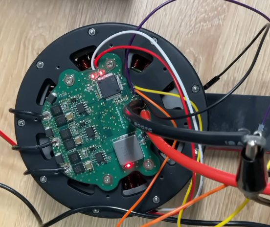
Failure to account for electrical, thermal, EMC, and manufacturing requirements during the design phase can lead to issues such as false overcurrent triggers, sensing drift, MOSFET overheating, controller resets, or even the destruction of power components. This guide outlines the core principles for designing and assembling motor controller PCBs, based on engineering best practices.
I. Defining Controller Architecture and Operating Conditions
PCB design should begin with a thorough analysis of system requirements, rather than jumping straight into layout. Key parameters to establish include the power input range, continuous and peak current levels, operating duty cycle, switching frequency, motor type, control strategy, ambient temperature, thermal management conditions, and any applicable safety or electromagnetic compatibility (EMC) standards.
Common controller architectures include H-bridges for brushed DC motors, three-phase inverters for brushless DC (BLDC) motors, and drives for permanent magnet synchronous motors (PMSM) utilizing Field-Oriented Control (FOC).
These architectures differ in terms of the number of power components required, current sensing methods, driving techniques, and protection strategies. Low-voltage, low-power applications may utilize driver ICs with integrated power stages, while higher-power designs typically employ discrete gate drivers paired with external MOSFETs or IGBT power modules.
During the schematic design phase, it is essential to define protection requirements—such as those for overcurrent, overvoltage, undervoltage, overtemperature, short circuits, reverse polarity, and motor stall. Furthermore, the system’s response to a fault must be clearly specified: should it disable the PWM signals, limit the current, or latch the fault state until a manual restart? Critical, high-speed fault responses should not rely solely on software polling; instead, they must be handled by the driver circuitry or dedicated hardware comparators to ensure an immediate reaction.
II. Planning PCB Partitioning and Stack-up
During the layout phase, the circuit can be divided into functional zones, such as power input and DC bus, power switching bridge, gate drivers, controller and clock circuitry, current/voltage sensing, and communication interfaces. Power loops should be kept as compact as possible, while control and sensing areas must be positioned away from high-noise switching nodes. Interfaces and connectors should be placed to facilitate assembly, routing, and future maintenance.
Partitioning is more than just segmenting the PCB into isolated copper regions. The critical aspect is to clearly define the origin of each current flow, its return path, and whether it traverses areas serving as references for sensitive signals. In particular, one must ensure that power return paths do not overlap with those used by sensitive signals—such as those for ADCs, encoders, or Hall-effect sensors—especially if the shared path is narrow or has unstable impedance.
The PCB stack-up must be determined by balancing factors such as current requirements, signal integrity, insulation, and cost.
Multi-layer boards allow for the use of solid reference planes to control return paths and provide low-impedance connections for power and ground. For high-current applications, it is also necessary to evaluate copper thickness, copper surface area, the current-carrying capacity of vias, and the temperature rise at board-edge connectors. Final parameters should be calculated based on actual current, board thickness, copper weight, ambient temperature, and the manufacturer’s capabilities; one should not rely solely on empirical rules of thumb for trace widths.
III. Optimizing Power Loops to Reduce Parasitic Inductance
The power stage is the core of a motor controller and the area most prone to issues in PCB design. During high-speed switching of MOSFETs, parasitic inductance—present in traces and component packages—interacts with changing currents to generate voltage spikes. This can lead to overvoltage, ringing, additional power losses, and electromagnetic interference (EMI).
Design efforts should prioritize minimizing the high-frequency commutation loop formed by the DC bus capacitors, power switching devices, and their respective return paths. High-frequency ceramic bypass capacitors should be placed as close as possible to the supply and return terminals of the power bridge. While large-capacity bus capacitors handle lower-frequency energy buffering, they cannot replace the high-frequency decoupling required immediately adjacent to the switching devices. As noted in TI’s motor driver layout guidelines, reducing the parasitic inductance between the bypass capacitors and the switching current path is generally more effective at suppressing voltage spikes.
Power devices should be placed as close as possible to their corresponding bus capacitors and gate drivers, while still allowing sufficient space for heatsinks, screws, insulation pads, and automated assembly processes. In a three-phase inverter, the phase nodes—which exhibit high voltage slew rates—should have their copper trace area minimized. These traces should not be routed over long distances through control areas, nor should they be positioned to create unnecessary coupling with sensitive signal lines. For high-voltage systems, creepage distances, clearances, insulation slots, and pollution degrees must also be evaluated in accordance with applicable safety standards.
When designing for high-current copper traces, one must look beyond mere trace width. Factors such as copper thickness, effective cross-sectional area, the number of vias, pad and connector interfaces, temperature rise, and the current’s distribution path across the plane must all be considered. In designs where multiple MOSFETs are connected in parallel, it is essential to ensure that the electrical paths and thermal conditions for each branch are as uniform as possible; this prevents any single branch from carrying excessive current due to lower impedance.
IV. Gate Drive Layout Determines Switching Quality
Gate drivers are responsible for rapidly charging and discharging the gate capacitance of MOSFETs. Their layout directly influences switching losses, ringing, and the risk of unintended turn-on. Drivers should be positioned as close as possible to their respective power devices, with gate traces kept short and direct; the forward and return paths of the drive loop should be routed in close proximity. If discrete gate resistors are used, they should generally be placed near the MOSFET gate. The decision to employ separate resistors for turn-on and turn-off should be based on device parameters, switching waveforms, and EMI test results.
Bootstrap capacitors and gate-driver supply decoupling capacitors should be placed close to the corresponding driver pins to minimize the supply loop area. Pin assignments for high-side drivers, low-side drivers, and switching nodes must strictly adhere to the chip’s datasheet; traces should not be arbitrarily lengthened or rerouted simply for the sake of layout convenience. Infineon’s gate-drive layout guidelines also note that fast-switching devices are sensitive to PCB parasitic parameters, necessitating careful, specialized planning of the drive loop.
Once the layout is complete, verify that the gate loops are not positioned too close to phase nodes, clock lines, reset lines, or communication traces. When necessary, trade-offs between efficiency and EMI can be managed through gate resistance, drive strength, snubber networks, or switching speed control; however, these measures should not be viewed as a substitute for correcting a flawed PCB layout.
V. Current Sensing and Analog Signal Routing
Current sensing is critical for torque control, current limiting, short-circuit protection, and the accuracy of FOC (Field-Oriented Control) algorithms. Common methods include single-shunt DC-bus sensing, dual- or triple-shunt phase-current sensing, and detection via the voltage drop across a conducting power device. The chosen sensing scheme should account for the control algorithm, PWM timing, low-speed performance, cost, and protection response time.
When using shunt resistors, a Kelvin (four-wire) connection is preferred: the load current flows through the power terminals of the resistor, while the sensing signal is tapped from dedicated, separate pads. This prevents the voltage drop across high-current copper traces from being superimposed onto the low-level sensing signal. Sensing amplifiers should be placed as close to the shunt resistors as possible; differential input traces should be routed as symmetric pairs, kept well away from gate drivers, switching nodes, and motor phase lines. Filter component values (resistance, capacitance, and cutoff frequency) must be evaluated in conjunction with amplifier stability, ADC sampling timing, and control-loop bandwidth—simply increasing the capacitance is not an appropriate solution.
For Hall sensors, encoders, temperature sensors, and DC-bus voltage sensing, careful attention must be paid to reference grounds, input protection, and filtering. Before analog signals reach the MCU, ensure their voltage ranges comply with ADC specifications, and account for potential fault conditions such as open circuits, short circuits, noise spikes, or sensor power supply anomalies. During debugging, it is advisable to simultaneously observe the sensing waveforms, PWM edges, and motor phase currents to determine whether any errors stem from hardware layout, sampling timing, or the control software.
VI. Grounding, EMC, and Signal Isolation
Grounding design should focus on facilitating current return paths, rather than simply segmenting all ground planes. The configuration for connecting controller, driver, and power grounds should be determined based on the chip manufacturer’s reference design, the current-sensing topology, and the chosen isolation scheme. For many low-voltage drivers, maintaining a continuous, low-impedance ground plane—while directing high-current return paths through designated areas—typically yields more predictable results than arbitrarily partitioning the ground plane.
Signals such as PWM, SPI, UART, encoder inputs, and crystal oscillator traces should be routed away from high-$dv/dt$ phase nodes and high-current loops. When routing across different regions, ensure that the reference plane remains continuous; signals must not cross gaps in the ground plane. At connector interfaces, consider implementing common-mode filtering, TVS diodes, shielding, and chassis grounding, depending on cable length and the application environment.
Specific filtering components and grounding points should be determined through system-level testing; it is not advisable to indiscriminately add ferrite beads, capacitors, or common-mode chokes without empirical measurement.
For systems involving high-voltage motors, long cables, or complex industrial environments, it is critical to address electrical isolation, surge immunity, electrostatic discharge (ESD), and conducted/radiated emissions. Once the PCB design is complete, EMC verification must be performed using the actual wiring harnesses, enclosure, motor, and grounding configuration, as these elements significantly influence final performance.
VII. Thermal Management and Component Selection
MOSFETs, gate drivers, shunt resistors, rectifiers, and power ICs all generate heat. Thermal design should be integrated into the component selection phase, with an evaluation of conduction losses, switching losses, reverse-recovery losses, and temperature rise under various operating conditions. Decisions should not be based solely on a component’s nominal maximum current, as such ratings are typically established under specific cooling conditions. In practice, the junction temperature on a PCB is also influenced by copper area, package thermal resistance, airflow, and the enclosure.
Heat dissipation can be improved through the use of large copper pours, thermal vias, exposed thermal pads, metal-core PCBs, or external heatsinks. The number and placement of thermal vias should be coordinated with the soldering process to prevent solder wicking into the vias, which could compromise the integrity of the solder joints. Sufficient space for heat dissipation must be maintained around high-power components. Furthermore, ensure that capacitors, current-sensing resistors, and temperature-sensitive components are not placed in direct contact with heat sources. If thermal pads, insulating sheets, or mechanical fasteners (such as screws) are used, their voltage withstand rating, clamping force, and long-term reliability must be verified.
While thermal simulation helps identify potential risks, it cannot replace actual physical testing. Temperatures of critical components should be measured on prototypes under representative operating conditions—including maximum ambient temperature, continuous rated load, peak load, frequent start-stop cycles, and locked-rotor scenarios. Additionally, design margins should be incorporated to account for aging, dust accumulation, and variations in thermal management conditions.
VIII. PCB Assembly and Manufacturing Quality Control
Before entering the manufacturing phase, Design for Manufacturing (DFM) and Design for Assembly (DFA) checks must be completed. Verify component packages, polarity, pad dimensions, stencil apertures, component spacing, test points, connector orientation, and mechanical mounting holes. Simultaneously, ensure consistency across the Bill of Materials (BOM), coordinate files, placement diagrams, Gerber/ODB++ data, and assembly instructions. For high-current terminals, power components, and heatsink structures, confirm the process capabilities with the PCB and PCBA manufacturers in advance.
SMT assembly typically involves solder paste printing, component placement, reflow soldering, Automated Optical Inspection (AOI), and, where necessary, X-ray inspection. Pads with high thermal mass, components with bottom-side thermal pads, and large-sized connectors are prone to issues such as insufficient solder, voids, or uneven heating; therefore, stencil designs and reflow profiles should be adjusted according to the specific component packages and process requirements. For through-hole terminals, busbar connection points, and components subject to mechanical stress, particular attention must be paid to solder joint strength and securing methods.
Cleaning, conformal coating, and potting are not required for all motor controllers; their necessity should be determined based on factors such as ambient humidity, dust levels, potential for corrosion, thermal management requirements, and serviceability.
If a coating is applied, ensure that it does not contaminate connectors, test points, thermal contact surfaces, or areas where specific electrical clearance distances must be maintained. For assembly acceptance, refer to the applicable version of the IPC-A-610 standard. For soldering process requirements, establish inspection criteria by combining the IPC J-STD-001 standard with specific customer requirements; the former focuses on assembly acceptability, while the latter addresses the soldering process itself.
IX. Power-Up Debugging and Reliability Verification
Once the PCBA is assembled, do not immediately apply the rated voltage or connect a full load. First, check for short circuits, correct polarity, soldering quality, resistance values of critical power rails, and the power supply to the driver circuitry. Then, perform an initial power-up at a low voltage using a current-limited power supply to verify the auxiliary power supply, MCU startup, communication interfaces, and fault signaling. Subsequently, under no-load or safe, low-energy conditions, verify the PWM outputs, dead-time, gate drive waveforms, and the state of the high-side and low-side bridge arms. Only after confirming there is no risk of “shoot-through” (direct conduction) should you gradually increase the DC bus voltage and load.
Functional testing must cover steering, speed control, acceleration/deceleration, startup/stop sequences, stall or overload protection, current limiting, over-temperature response, and handling of under-voltage or over-voltage conditions. For FOC (Field-Oriented Control) controllers, it is also necessary to verify the consistency of phase current sampling, zero-point offset, sampling synchronization, and stability during low-speed operation. Throughout the testing process, simultaneously recording the DC bus voltage, current, temperatures of critical components, switching waveforms, and fault logs will significantly improve the efficiency of root-cause analysis.
For mass production validation, develop a test plan—including vibration, shock, temperature/humidity cycling, long-term operational life testing, and EMC testing—tailored to the product’s specific application. The goal is not to maximize the number of tests, but to ensure coverage of the actual operating environment and the most likely failure modes. If an anomaly occurs during testing, identify the root cause by analyzing the schematic, PCB return paths, thermal imaging, and waveforms; then, implement design revisions and conduct regression testing to confirm the issue has been resolved.
X. Common Design Pitfalls
First, determining trace widths based solely on current magnitude while neglecting copper thickness, vias, connectors, and temperature rise. Second, placing the driver too far from the MOSFETs, which results in an excessively long gate loop. Third, routing current-sampling traces in parallel with phase nodes, which introduces noise and causes jitter in current measurements. Fourth, arbitrarily cutting the ground plane, which forces return currents to take circuitous paths and increases electromagnetic interference. Fifth, functionality is verified only under no-load conditions, failing to account for scenarios such as motor stall, over-temperature, rapid acceleration/deceleration, and sustained full-load operation. Sixth, considerations regarding stencils, thermal management structures, and test points are often deferred until after the design phase, leading to costly rework or inconsistent quality during mass production.
These issues rarely stem from the inadequate performance of a single component; rather, they indicate a lack of a closed-loop integration between system design, PCB implementation, assembly processes, and verification workflows.
Conclusion
The reliability of a motor controller PCB depends on the synergistic design of the power loop, gate drive, current sensing, grounding and EMC, thermal management, and PCB assembly processes. Designers should base their work on real-world operating conditions and potential failure modes—minimizing high-frequency current loops and noise coupling during the layout phase, ensuring the manufacturability of solder joints and thermal structures during assembly, and systematically validating protection mechanisms, temperature rise, and electromagnetic compatibility during testing.
For applications such as industrial robots, power tools, drones, and new energy vehicles, it is highly recommended to involve teams specializing in circuit design, PCB manufacturing, PCB assembly, mechanical/thermal design, and testing in a collaborative review process from the earliest stages of a project. Through rigorous schematic checks, layout reviews, prototype testing, and process control during mass production, a motor controller can evolve from merely “functional” to a solution that is stable, reliably manufacturable, and durable for long-term use.