Face recognition systems are now widely used in smart access control, time and attendance terminals, intelligent security, financial payment systems, and high-end industrial automation equipment.
These systems typically integrate complex functions such as image acquisition, deep-learning-based feature extraction, comparison processing, and external communication. As the hardware foundation, the design quality of the printed circuit board (PCB) directly determines the system’s stability, recognition speed, interference resistance, and mass-production yield.
This article explores PCB design solutions for face recognition systems, covering aspects such as system architecture, core circuit layout, high-speed signal integrity, and power integrity.
I. System Architecture and Selection of Core Components
The overall architecture of a face recognition system (PCBA) consists primarily of a main control unit, an image acquisition unit, storage and memory units, a power management unit, and peripheral communication interfaces. A well-planned architecture is the prerequisite for a successful PCB layout.
Main Control and AI Processing Unit: Typically utilizes a high-performance embedded AI processor (such as the Rockchip RK3399, HiSilicon series chips, or heterogeneous NPU-based chips) to execute deep-learning convolutional neural networks (CNNs) and facial feature comparison algorithms.
Image Acquisition Unit: Supports binocular infrared (IR) and visible-light (RGB) camera modules, utilizing MIPI-CSI bus interfaces to enable liveness detection and accurate recognition in low-light or nighttime conditions.
Storage Unit: Includes high-speed LPDDR4/DDR3 memory and eMMC storage chips, ensuring smooth operation of the operating system and rapid access to facial feature databases capable of handling tens of thousands of records.
Communication and Control Interfaces: Integrates Ethernet, Wi-Fi/Bluetooth modules, Wiegand protocol support, relay controls, and USB interfaces, facilitating data exchange with turnstiles, electronic locks, and cloud-based backend systems.
II. PCB Stack-up Design and Lamination Planning
The mainboard of a face recognition system typically integrates high-speed processors, DDR memory, and high-speed MIPI image interfaces, making it a classic example of a high-density, mixed-signal system. Layer Stackup Selection: A 6-layer or 8-layer PCB design is recommended (a typical 6-layer stackup: Top Signal – GND – Inner Signal/Power – Inner Power/Signal – GND – Bottom Signal). Incorporating a solid internal ground plane (GND) provides a low-impedance return path for high-speed signals, effectively suppressing electromagnetic interference (EMI).
Impedance Control:
Single-ended Impedance: Controlled at 50Ω ± 10%.
Differential Impedance: For differential pairs—such as those used for USB, MIPI, or Ethernet—the differential impedance must be strictly controlled at 100Ω ± 10%.
III. Key Circuit Layout and Routing Design
Image Acquisition and MIPI Interface Layout
Camera Module: The MIPI bus operates at high frequencies and consists of critical, sensitive signals. During PCB layout, MIPI differential pairs must be routed closely together and precisely matched in length, with tolerances kept within the mil range.
Isolation from Interference: MIPI traces should be kept away from switching power supply ICs, inductors, and high-current traces to prevent issues such as streaking noise in images or false triggering.
DDR Memory Area Design
Compact Layout: The distance between the main control chip (SoC) and the LPDDR memory should be minimized. Both components should be placed on the same side of the PCB to reduce the number of vias.
Length Matching and Topology: Address, control, and data lines must be routed with serpentine traces to ensure precise length matching, as specified in the chip’s datasheet, to guarantee timing synchronization.
Power Integrity (PI) and Decoupling Design
Multi-rail Power Output: AI SoCs typically require multiple voltage rails (e.g., Core, VDD_IO, DDR supply, etc.). Power modules should utilize high-efficiency DC-DC step-down (buck) converters.
Capacitor Configuration: Large-capacity energy-storage capacitors (e.g., 10uF/22uF) and high-frequency decoupling capacitors (e.g., 0.1uF/0.01uF) must be strategically placed near the power pins of each chip. This configuration filters out high-frequency noise and ensures voltage stability for the core processor during transient, high-load operations.
Thermal Design and Heat Dissipation Layout
During continuous operation or intensive AI inference tasks, the main control chip and power management ICs in a facial recognition terminal generate significant heat.
In the PCB design, a large thermal pad should be incorporated beneath the chips (such as those in QFN or BGA packages), accompanied by an array of thermal vias. This facilitates the rapid transfer of heat to internal layers or the copper foil on the opposite side of the board; external heatsinks may be added if necessary.
IV. Signal Integrity (SI) and Electromagnetic Compatibility (EMC) Design
Facial recognition systems integrate high-frequency image transmission, high-speed CPU/DDR clock signals, and wireless communication modules. As high-density mixed-signal boards, they are highly susceptible to electromagnetic interference (EMI) and signal distortion.
Signal Integrity (SI) and Impedance Control:
Protection of High-Speed Traces: For MIPI-CSI, USB 3.0, and DDR data lines, a continuous reference plane must be maintained along the entire signal path; crossing splits or gaps in the reference plane is strictly prohibited. If a trace must cross between different power domains, bypass capacitors or “stitching vias” should be added nearby to provide a low-impedance return path for high-frequency signals.
Crosstalk Mitigation: High-speed signal traces must adhere to the “3W rule” (the distance between the centers of two traces should be at least three times the trace width). For highly sensitive circuits—such as crystal oscillator circuits and high-frequency clock lines—the “5W rule” should be applied, supplemented by “ground shielding” (surrounding the traces with ground copper) to prevent signal crosstalk caused by excessively long parallel routing. Electromagnetic Compatibility (EMC) and Electrostatic Discharge (ESD) Protection:
Interface ESD Protection: Face recognition terminals are often deployed in outdoor or semi-outdoor environments. Interfaces—such as camera ports, relay terminals, USB ports, and power inputs—are highly susceptible to electrostatic discharge (ESD) strikes. Low-capacitance TVS (Transient Voltage Suppressor) diodes must be placed at the first stage of every external interface. These TVS components should be positioned as close to the interface connectors as possible to ensure that electrostatic pulses are rapidly shunted away before they can reach the core circuitry.
Power and Ground Isolation: Utilize single-point grounding or ferrite bead isolation to effectively separate the sensitive analog ground (AGND) of the camera front-end from the high-noise digital ground (DGND) of the main controller. This prevents digital switching noise from contaminating the image signals.
V. Design for Manufacturing (DFM) and Design for Testability (DFT)
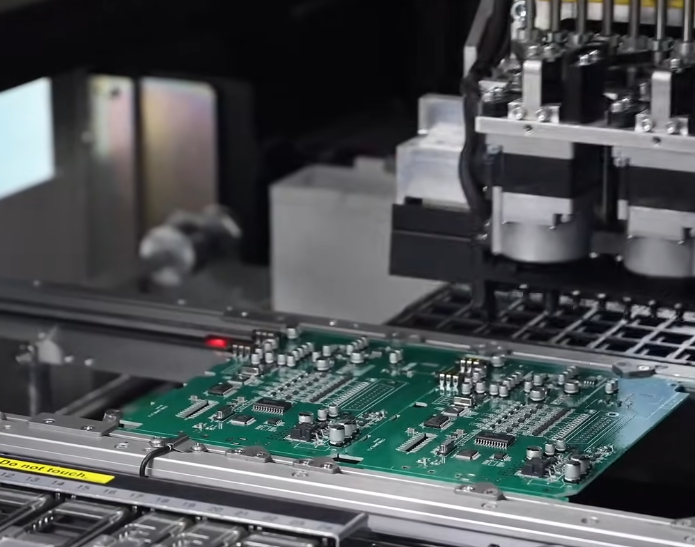
An excellent PCB design must go beyond meeting electrical performance requirements; it must also ensure high manufacturability and comprehensive test coverage, which are essential for achieving high yields during SMT (Surface Mount Technology) assembly and reducing production costs.
DFM (Design for Manufacturing) Guidelines:
BGA and High-Density Pads: AI main controllers and memory chips often utilize BGA packages with a pitch of less than 0.8mm. In such designs, “via-in-pad” technology—combined with resin-plugged vias and an ENIG (Electroless Nickel Immersion Gold) surface finish—should be employed to prevent soldering defects such as “cold” (weak) joints or solder wicking (loss of solder from the pad).
Component Spacing and Thermal Balance: For miniature 0402/0201 SMD components, trace widths on both sides of the pads should be kept symmetrical to avoid uneven heat dissipation, which can lead to “tombstoning” defects. Additionally, a safety margin of at least 3mm should be maintained between large components and the board edges to prevent mechanical stress—occurring during panel separation (via V-cutting or stamping)—from damaging the chips. DFT (Design for Testability) Specifications:
Test Point Provisioning: Strategically incorporate test points on the bottom layer of the PCB for power rails, critical control signals, and SWD/JTAG programming/debugging interfaces. A minimum spacing of 1.0 mm (40 mil) between test points is recommended to facilitate In-Circuit Testing (ICT) and Functional Testing (FCT) on the production line, significantly enhancing quality inspection efficiency during mass production.
VI. Conclusion
The PCB design for a facial recognition system is a complex engineering endeavor that encompasses high-speed digital circuitry, analog image transmission, power management, and structural thermal management. Any oversight in these areas can lead to system freezes, excessive image noise, or a decline in recognition accuracy.
As a leading PCB manufacturer and PCBA contract manufacturer in China—with deep expertise in electronic manufacturing and smart hardware—KingTop Technology leverages the robust electronics supply chain in Shenzhen. Backed by extensive technical experience in high-end PCB design, high-precision multi-layer board fabrication, and SMT (Surface Mount Technology) assembly, we provide global clients with comprehensive, one-stop Electronic Manufacturing Services (EMS). Our offerings range from schematic review and high-density PCB layout to DFM (Design for Manufacturing) optimization and the delivery of finished PCBA products.
Adhering to rigorous international industry standards, and utilizing the exceptional quality and efficient delivery capabilities of “Intelligent Manufacturing in China,” we ensure that every facial recognition motherboard achieves an optimal balance of performance, stability, and cost—empowering your smart hardware products to swiftly capture opportunities in the global market.