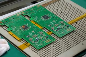
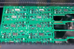
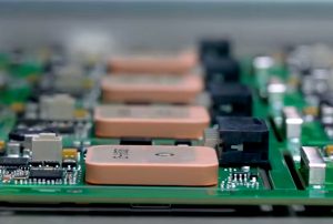
Driven by the Internet of Things (IoT), smart manufacturing, modern logistics, and operations in extreme environments, industrial PDAs (handheld terminals/data collectors) have evolved from simple barcode scanning tools into comprehensive mobile terminals integrating multi-mode communication, high-precision positioning, machine vision, and powerful edge computing capabilities.
Unlike consumer smartphones, which prioritize slimness and cost-effectiveness, industrial PDAs demand high reliability, environmental adaptability, longevity, and extreme resistance to drops and vibrations.
Underpinning these requirements, PCB (Printed Circuit Board) design and PCBA (Printed Circuit Board Assembly) manufacturing processes serve as the fundamental pillars determining the performance limits of industrial PDAs.
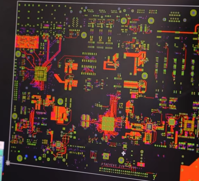
This article provides an in-depth analysis of the hardware engineering implementation of industrial PDAs, covering four key dimensions: system architecture, critical PCB design technologies, PCBA manufacturing processes, and quality control.
I. Industrial PDA System Architecture and PCB Functional Partitioning
The internal space of an industrial PDA is extremely constrained (typically only a dozen millimeters thick, yet housing a battery, high-power scanning engine, RF antennas, and both main and sub-boards), resulting in a highly integrated system architecture.
Core System Components
Computing and Storage Core: Industrial-grade SoCs (e.g., Qualcomm Snapdragon industrial platforms, MediaTek IoT chips), LPDDR4x/LPDDR5 memory, and eMMC/UFS flash storage.
Wireless Communication Modules: 4G/5G cellular networks, Wi-Fi 6/6E, Bluetooth 5.2, NFC, and high-precision GPS/GNSS positioning.
Data Acquisition Modules: 1D/2D barcode scanning engines (laser or imager-based), UHF RFID modules, and fingerprint or iris recognition modules.
Power Management System (PMIC): Multi-channel high-efficiency DC-DC converters, lithium battery charge/discharge protection, fast-charging protocol chips, and dynamic thermal management.
Human-Machine Interaction and Interfaces: High-durability industrial touchscreen, industrial-grade buttons, multifunctional Pogo pins (for dock charging and data transmission), and USB Type-C port.
PCB Functional Partitioning Principles
Since high-frequency RF signals, high-speed digital signals, sensitive analog signals, and high-current power circuits coexist on a single compact PCB, rational functional partitioning is the first step toward ensuring electromagnetic compatibility (EMC):
RF Section: Located near the antenna interface edge to ensure impedance matching (typically 50 ohms) and isolation from noise sources.
Digital High-Speed Section: SoC and memory are placed in close proximity to minimize trace lengths and reduce parasitic inductance.
Power Section: High-current components such as PMICs, inductors, and MOSFETs are grouped together, with a focus on heat dissipation and ground plane integrity.
Interface & Protection Section: TVS diode arrays are positioned at external interfaces to immediately absorb electrostatic discharge (ESD) and surge energy.
II. Four Core Technical Challenges in Industrial PDA PCB Design
PCB design for industrial PDAs tests not only circuit performance but also the ability to manage space, heat, and mechanical stress under extreme constraints.
High-Density Interconnect (HDI) and Micro-via Technology
Due to extremely high component density, traditional through-hole PCBs can no longer meet routing requirements. Industrial PDAs commonly utilize HDI PCB designs:
Stack-up Selection: Second- or third-order HDI boards are typically used (e.g., 1+2+1 or 2+4+2 structures), employing laser blind vias for interlayer interconnection.
Via-in-Pad (VIPPO): Vias are drilled directly beneath BGA pads and filled via plating; this significantly saves routing space, shortens high-frequency signal paths, and reduces parasitic inductance. 2. High-Speed Signal Integrity (SI) and Power Integrity (PI)
DDR Bus Optimization: Memory traces require strict length matching (using serpentine routing) and precise differential impedance control (50Ω single-ended, 100Ω differential), while maintaining separation from sources of interference.
Power Plane Partitioning and Decoupling: To support the SoC core’s multi-rail, low-voltage, high-current power requirements, the PCB design must utilize large copper pour areas on the bottom layer for power delivery. Additionally, ceramic capacitors of varying values (e.g., 0.1 μF, 1 μF, 10 μF) should be strategically placed near each power pin to filter high-frequency noise and prevent voltage droop (IR Drop).
Thermal Design and Simulation (Thermal Management)
Industrial PDAs generate significant heat during continuous high-intensity scanning, 5G communication, or AI edge computing operations; however, their fully sealed enclosures (often requiring IP65, IP67, or even IP68 ratings) render convective air cooling largely ineffective.
Thermal Path Design: During PCB layout, dense arrays of thermal vias must be placed directly beneath major heat-generating components—such as the SoC and PMIC—to rapidly conduct heat to the internal metal mid-frame or graphite heat spreaders.
Copper Pour Optimization: Increasing the copper thickness of internal power/ground layers (e.g., from 1 oz to 2 oz) not only supports higher current loads but also facilitates excellent heat spreading.
Mechanical Shock Resistance and ESD (Electrostatic Discharge) Design
Drop and Shock Resistance: Industrial PDAs frequently face the risk of free-fall drops from heights of 1.5 meters or more in warehouse or construction site environments. The PCB design should avoid excessive rigidity; sensitive components located near the edges (such as ceramic capacitors and crystal oscillators) must be kept away from areas prone to high-stress deformation—such as the center of the mainboard or locations near screw mounting points—to prevent solder joint fractures caused by PCB flexing.
Electrostatic Discharge (ESD) Protection: External interfaces (USB ports, Pogo pins, buttons) are high-risk areas for ESD events. Regarding PCB layout, ESD protection devices must be placed immediately adjacent to the interfaces to ensure the shortest possible ESD discharge path and minimal ground impedance.
III. Industrial PDA PCBA Manufacturing and Assembly Processes
Once the PCB design is complete, successfully transforming it into physical hardware with a high yield relies on advanced PCBA (Printed Circuit Board Assembly) manufacturing processes.
SMT (Surface Mount Technology) Process for Precision Components
Industrial PDA boards are densely populated with miniature components (such as resistors and capacitors in 0201 or 01005 packages, as well as fine-pitch BGA and QFN chips).
Stencil Design: For BGA and fine-pitch QFN components, nano-coated or electropolished stencils are used to precisely control solder paste release, thereby preventing bridging or insufficient solder.
Reflow Profile Optimization: The temperature zone settings of the reflow oven are critical. Temperature gradients across the preheat, soak, reflow, and cooling zones must be gradual to avoid thermal shock, which could cause internal BGA voiding or PCB warping. Industry standards typically require BGA solder joint voiding rates to be kept below 15%.
Mixed Assembly Process for Odd-form Components and Structural Parts
Industrial PDAs contain not only SMD components but also many parts that cannot be assembled via standard SMT processes:
Pogo pins and battery connectors: These often utilize special high-temperature plastics and are assembled via manual insertion (THT), selective wave soldering, or laser welding.
Mounting of scanning modules and camera modules: This involves the crimping of precision FPC (Flexible Printed Circuit) connectors and reinforcement using adhesive dispensing. 3. Conformal Coating & Underfill
To withstand extreme industrial environments (such as condensation in cold-chain logistics, or oil and dust in factories):
Underfill: Capillary underfill material is injected beneath main chips (e.g., SoCs, high-capacity memory) and cured. This creates a mechanical anchoring effect, significantly enhancing resistance to drops and thermal cycling.
Conformal Coating: After PCB assembly, the entire board undergoes full or selective coating with acrylic resin or polyurethane conformal coating to provide protection against moisture, salt spray, and mold.
IV. Quality Inspection and Reliability Verification
Before leaving the factory, the industrial PDA’s PCBA must pass rigorous quality inspection checkpoints to ensure absolute reliability.
SPI (Solder Paste Inspection) & AOI (Automated Optical Inspection): Comprehensive inspections are conducted before and after printing and reflow soldering to detect surface defects such as insufficient or excessive solder, misalignment, and “tombstoning.”
X-Ray Inspection: Used to examine solder quality and void ratios for bottom-terminated packages like BGA and QFN.
ICT / FCT (In-Circuit Testing & Functional Testing): Fully automated batch testing of the entire board’s electrical performance, RF specifications, and barcode scanning capabilities using bed-of-nails fixtures or test jigs.
Environmental Reliability Testing:
High/Low-Temperature Burn-in: Long-duration powered-on aging tests conducted in chambers with extreme temperature ranges (-40°C to +85°C).
Vibration and Drop Testing: Simulations of vehicle-induced jolts and everyday drop scenarios to verify the mechanical strength of the PCB and solder joints.
Conclusion
The PCB design and PCBA manufacturing of industrial PDAs represent a system-level engineering process that integrates microelectronics, electromagnetic field theory, thermodynamics, and mechanical engineering. Every minute via, the impedance of every differential pair, and the process parameters of every solder joint directly impact the device’s operational viability—whether on a production line, in a parcel sorting center, or in the field during surveying operations. With the widespread adoption of new technologies such as artificial intelligence, edge computing, and 5G-R (RedCap), future industrial PDAs are set to become increasingly lightweight and intelligent.
This evolution places higher demands on PCB design, requiring the integration of high-density heterogeneous computing units and complex RF front-ends within a compact footprint. Only by continuously refining high-reliability PCB designs and advanced assembly processes can a rock-solid hardware foundation be established for industrial-grade smart terminals.
KingTop Technology’s excellence in industrial PDA hardware: As a leading provider of smart hardware solutions, KingTop Technology possesses deep technical expertise in industrial PDA PCB design and PCBA manufacturing.
By implementing advanced HDI micro-via manufacturing processes, rigorous high-speed signal integrity (SI) and power integrity (PI) simulations, and comprehensive Design for Manufacturability (DFM) standards, KingTop Technology has successfully overcome the electromagnetic interference challenges associated with co-locating multi-mode RF front-ends and high-density computing units. Its products maintain exceptional stability and ultra-low failure rates even under harsh operating conditions involving extreme temperatures, intense vibration, and high-impact drops.
Looking ahead, KingTop Technology will continue to collaborate with global partners, leveraging rock-solid hardware quality to drive the evolution of industrial-grade smart terminals toward greater portability and intelligence.