Amidst the current wave of intelligent technology and the rapid evolution of Embodied AI, facial recognition robots have evolved from simple identity verification terminals into sophisticated intelligent systems that integrate computer vision, edge computing, multimodal emotional interaction, and complex motion control.
As the physical foundation housing the robot’s “visual center” and “motion brain,” the design and manufacturing quality of the printed circuit board (PCB) directly determine the system’s computational performance, signal integrity, image acquisition stability, and long-term reliability in demanding industrial environments.
Because facial recognition robots integrate high-density AI core boards, multiple MIPI high-definition cameras, infrared structured light or area-scan ToF depth modules, motor drivers, and wireless communication modules, their PCB hardware architecture presents a complex profile characterized by intertwined signals, high-speed/high-capacity storage, low-power energy management, and significant electromagnetic compatibility (EMC) challenges.
To ensure efficient and stable system operation, deep, multi-dimensional collaboration—spanning architecture planning, high-speed routing, interference-resistant design, thermal management, and advanced manufacturing processes—is essential to create a hardware foundation that delivers both high performance and high reliability.
I. Hardware System Architecture and PCB Layer Planning for Facial Recognition Robots
The hardware systems of facial recognition robots typically employ either a distributed architecture or a highly integrated single-board design comprising a heterogeneous multi-core processor, a dedicated AI acceleration card/NPU, a vision sensor array, and a motion control unit. Accommodating complex circuit interconnections while suppressing electromagnetic crosstalk makes PCB layer planning and stack-up design a critical initial phase of hardware development.
Integrated Architecture of Core Computing Mainboard and Vision Modules
Modern facial recognition terminals commonly utilize high-performance computing platforms such as the NVIDIA Jetson series or the RK3588. These chips integrate multi-core CPUs, GPUs, and NPUs capable of 6 TOPS to over 275 TOPS, supporting real-time input from multiple 4K cameras and real-time facial recognition matching.
The PCB architecture is typically divided into a core board (SoC + LPDDR + eMMC/UFS) and a baseboard (peripheral interfaces, motor drivers, power conversion, and audio/display interfaces). The baseboard design must balance rigid mechanical strength with high-density signal escape capabilities.
Vision front-end modules (such as RGB binocular cameras, IR cameras, and 3D depth cameras) connect to the mainboard via high-speed serial interfaces; the mainboard PCB must provide high-bandwidth, low-loss transmission channels for these high-speed video streams.
Multilayer PCB Stack-up Design and Impedance Control
To handle complex routing densities and high-frequency signals, HDI (High-Density Interconnect) structures with 8, 10, or even 12 layers are commonly employed. Taking a typical 8-layer board as an example (e.g., Signal-GND-Signal-Power-Power-Signal-GND-Signal), a strategic stack-up arrangement ensures that every high-speed signal layer has an adjacent reference ground plane (image plane).
Strict impedance control is crucial for ensuring high-speed data integrity. Single-ended trace impedance is typically designed at 50 Ω, while differential pairs (such as MIPI CSI-2, USB 3.0/3.1, PCIe, and Ethernet) require precise control at 85 Ω or 100 Ω. Stack-up design utilizes high-frequency, high-speed materials with stable dielectric constants and low dissipation factors (Df)—such as mid/high-Tg FR-4 or Megtron series materials—and employs field solvers (like Polar Si9000) to precisely calculate trace width, spacing, and dielectric thickness.
Co-simulation of Signal Integrity (SI) and Power Integrity (PI)
Pre- and post-layout simulation processes must be integrated during the initial design phase. Power Distribution Network (PDN) impedance analysis is conducted to address transient current spikes that may occur during dynamic facial capture operations by the robot. By strategically placing surface-mount ceramic capacitors of varying values (e.g., 10 μF, 1.0 μF, 0.1 μF) at critical PCB nodes—specifically the power supply inputs for AI processor cores and DRAM—a wideband decoupling network is created. This keeps the Power Distribution Network (PDN) impedance below the target level, preventing logic errors caused by ground bounce noise.
II. The Art of High-Speed PCB Routing for Edge Computing and Machine Vision
Facial recognition robots handle massive visual data throughput; the process—ranging from raw image capture by cameras to feature extraction and matching—involves extensive high-speed serial and parallel bus interactions. PCB routing is not merely about establishing connections; it is about the precise guidance of electromagnetic energy.
MIPI CSI-2/DSI High-Speed Differential Pair Routing and Length Matching
Robots typically employ two to four MIPI cameras for multi-angle facial capture. MIPI CSI-2 interfaces operate at extremely high frequencies and are highly sensitive to timing jitter and phase skew.
Length Matching Specifications: Intra-pair skew (the length difference between the two conductors within a single differential pair) must typically be strictly controlled within ±2 mils (approx. 0.05 mm), while inter-pair skew (length mismatch between different differential pairs) must be kept within ±10 mils.
Routing Geometry Rules: All MIPI differential lines must maintain strict spacing (adhering to the “3W rule”—where the center-to-center distance is three times the trace width—to minimize edge crosstalk) and strictly avoid routing across reference plane splits. When traces change layers, a ground via must be placed near the signal via to ensure a continuous return current path.
DDR4/LPDDR5 High-Speed Memory Bus Topology and Crosstalk Suppression
AI inference requires high-capacity, high-bandwidth memory support. As mainstream memory solutions, LPDDR4 and LPDDR5 offer data transfer rates reaching several thousand Mbps. Topology Design: Command/Address signals typically utilize tree or daisy-chain topologies, whereas data lines (DQ/DQS) employ point-to-point direct connections.
Routing and Impedance: Impedance is controlled at 40 Ω–50 Ω for single-ended data lines and 100 Ω for differential clock lines. Routing must maintain clearance from high-frequency switching power supply inductors and high-current motor drive traces to prevent noise injection via low-frequency magnetic field coupling.
PCIe Gen3/Gen4/Gen5 High-Speed Bus Routing Specifications and Return Path Optimization
The PCIe bus serves as a critical backbone when robots are equipped with high-performance edge computing cards or external AI acceleration modules.
High-speed serial buses (such as PCIe TX/RX differential pairs) must utilize symmetrical, smooth arc-shaped corners (right-angle or acute-angle routing is strictly prohibited; 135° obtuse angles or arc transitions are recommended).
They should be routed at a distance of at least three times the dielectric thickness from the board edge to minimize edge radiation effects. Additionally, a continuous reference ground plane must be maintained beneath the differential pairs, and crossing over any slots or voids is strictly prohibited.
III. Interference-Resistant Design for Cameras and Multispectral Sensors
Practical facial recognition applications face challenges such as complex lighting conditions, backlighting, low-light environments, and spoofing attacks (e.g., photo or mask attacks). Consequently, multispectral fusion solutions—combining RGB binocular cameras with Near-Infrared (NIR) illuminators and structured light or Time-of-Flight (ToF) depth sensors—are frequently employed. Since analog small-signal circuits and high-speed digital signals coexist on the same PCB, interference-resistant design is crucial.
Image Sensor (CIS) Analog/Digital Ground Isolation and Mixed-Signal Processing
The photosensitive element (CMOS Image Sensor) within the camera module is extremely sensitive to power supply noise and ground noise.
In PCB design, strict isolation using ferrite beads and LC filters is required between sensitive analog power rails (AVDD) and digital power rails (DVDD, DOVDD).
Rational Planning of Analog Ground (AGND) and Digital Ground (DGND)
Analog and digital grounds should be physically partitioned and ultimately connected at a single point (typically via a high-frequency ferrite bead or a low-impedance copper bridge). This prevents digital switching noise from coupling into the analog front-end, which could otherwise cause noise, ripple patterns, or color distortion in facial images.
Driver and Power Delivery Network for Infrared Structured Light/Area-Array ToF (Time-of-Flight) Modules
Structured light projectors or ToF light-emitting diodes (VCSELs) require the instantaneous release of high-intensity, high-current pulses (with peak currents reaching several amperes) during operation.
Such transient high currents can cause significant voltage drops (IR drop) along power traces. Consequently, power traces for VCSEL driver circuits must be designed with increased width (recommended width ≥ 40 mils or large-area copper pours). Additionally, a matrix of high-capacitance, low-ESR (Equivalent Series Resistance) ceramic capacitors should be placed near the driver chip to ensure the instantaneous supply of pulse current, thereby preventing the loss of depth information caused by insufficient optical output power.
Electromagnetic Shielding and Grounding Design for Noise-Sensitive Areas
RF modules (Wi-Fi/Bluetooth/5G), image processing cores, and high-speed clock generation circuits are primary sources of electromagnetic interference (EMI).
During PCB layout, pads for shielding frames must be reserved, and a dense array of shielding ground vias (via stitching) should be implemented on the ground layer (with via spacing less than 1/20 of the wavelength corresponding to the highest operating frequency). A metal shielding cover should be installed during final assembly to block coupling paths between radiated electromagnetic fields and sensitive circuits.
IV. PCB Design for Power and Thermal Management in Robots Operating in Complex Environments
Facial recognition robots typically utilize internal lithium battery packs or external DC power supplies. Operating in diverse environments—ranging from indoor commercial settings to semi-open outdoor scenarios—places rigorous demands on the power system’s conversion efficiency and stability, as well as the device’s overall thermal dissipation capabilities. Multi-rail Power (PMIC) Planning, High-Current Trace Design, and Copper Thickness Selection
Robotic systems incorporate multiple independent power rails, including supplies for the core board (0.8 V – 1.8 V), peripheral interfaces (3.3 V – 5 V), and motor drives (12 V – 24 V).
For high-current paths (such as motor drives and battery charge/discharge management circuits), temperature rise and current-carrying capacity must be calculated in accordance with the IPC-2152 standard.
For traces carrying currents exceeding 3 A, avoid using long, narrow conductors; instead, employ techniques such as parallel copper pours across multiple layers or exposed copper areas reinforced with solder. A copper thickness of 2 oz or even 3 oz is recommended for outer layers, while inner layers should maintain a minimum of 1 oz.
Thermal Design for Vision Processors and AI Accelerator Chips (Buried Vias, Thermal Pads, and Thermal Via Arrays)
High-performance AI chips exhibit extremely high power density during continuous facial feature extraction, with localized temperatures potentially exceeding 90°C. Failure to dissipate heat effectively can trigger thermal protection mechanisms, leading to clock throttling or system crashes.
PCB Thermal Optimization: Design a dense thermal via array (0.3 mm diameter, ~1.0 mm pitch) beneath the chip (in the thermal pad area) to rapidly conduct heat to large-area ground planes in the inner layers or to an aluminum heat-dissipation substrate at the bottom. For multi-layer HDI boards, copper-filled via technology allows for blind/buried thermal vias directly beneath the pads, significantly enhancing thermal conductivity.
Isolation Between Power Drive and Control Systems (Low-Voltage/High-Voltage Separation, Optocoupler Isolation, and Surge Protection)
Servos, brushless motors, or stepper motors in the robot chassis generate significant back-electromotive force (back-EMF) and conducted electromagnetic interference (EMI) during startup and shutdown. In PCB layout, the principle of “separating high-voltage/high-current circuits from low-voltage/sensitive circuits” must be strictly enforced by physically distancing the high-voltage/high-current power section from the low-voltage sensitive digital control section (maintaining a safety clearance of at least 2 mm to 3 mm). Electrical isolation between control signals and power outputs is achieved using high-speed optocouplers or digital isolators (such as the ISO series), while TVS diodes and varistors are installed at the interfaces to absorb electrostatic discharge (ESD) and surge energy.
V. Manufacturing Process Challenges and High-Quality PCBA Production Control
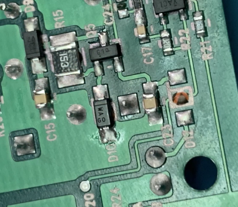
The flawless realization of a design depends on exquisite manufacturing processes. Due to their high integration and fine-pitch component packaging, PCBs for facial recognition robots demand extremely high precision in manufacturing and assembly (PCBA).
Selection of High-Density Interconnect (HDI) Materials and Blind/Buried Via Processes
Modern robot motherboards typically utilize 1+N+1 or 2+N+2 sequential HDI structures. Laser microvias generally have diameters ranging from 0.075 mm to 0.1 mm.
During manufacturing, strict control over lamination registration accuracy and dielectric layer thickness uniformity is essential. Pulse plating via-filling technology is employed to ensure uniform copper thickness within blind vias, thereby preventing thermal stress-induced fractures caused by plating defects.
Fine-Pitch BGA Soldering, Reflow Profile Optimization, and Stencil Design
AI main chips and LPDDR memory modules often utilize fine-pitch BGA packaging (with pitches as fine as 0.4 mm or 0.35 mm).
Stencil Optimization: For fine-pitch BGA pads, nano-coated stencils and laser-cut step stencils are used to precisely control solder paste release, preventing defects such as bridging or non-wetted/cold solder joints.
Reflow Profile Settings: Based on the characteristics of Sn-Ag-Cu (SAC305) lead-free solder, the preheat, soak, reflow, and cooling zones are scientifically configured. Peak temperatures are maintained between 240°C and 245°C with optimized reflow duration to ensure uniform Intermetallic Compound (IMC) layer growth, thereby maximizing drop-test reliability and thermal fatigue resistance.
Design for Manufacturability (DFM) Specifications and Reliability Testing (AOI, X-Ray, ESS)
Before generating Gerber files for the PCB design, a comprehensive DFM review is mandatory. This covers test point coverage, component spacing, panelization schemes, and the design of panelization tooling rails.
Following PCBA production, multiple rigorous quality inspections must be implemented:
AOI (Automated Optical Inspection): Checks for component misalignment, missing components, reversed polarity, and solder paste printing quality.
X-Ray Inspection: Utilizes 3D transmission imaging for bottom-terminated components (such as BGA and QFN) to ensure that internal solder joint void rates remain below industry standards (typically requiring <15% void rate for a single joint and <20% for the total area).
ESS (Environmental Stress Screening): Subjects mass-produced robot circuit boards to high/low-temperature cycling, burn-in testing, and vibration testing. This process filters out potential failures early on, ensuring exceptional product stability across diverse and complex application scenarios.
Conclusion
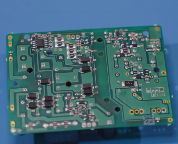
The PCB design and manufacturing process for facial recognition robots is a systematic undertaking that integrates microelectronics, high-speed circuit theory, electromagnetic compatibility (EMC) engineering, and advanced manufacturing technologies.
Only through end-to-end control—spanning initial system architecture, rigorous high-speed signal routing, multi-dimensional interference suppression, and thermal design, all the way to precision manufacturing and stringent testing—can the robot’s hardware system achieve superior performance in complex environments, characterized by ultra-low error rates, rapid response times, and exceptional longevity.