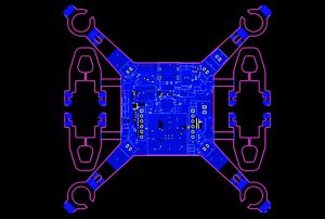
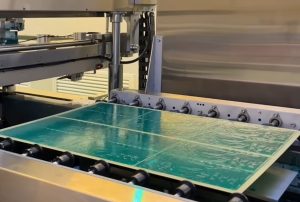
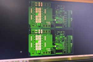
With the explosive growth of global Unmanned Aerial Vehicle (UAV) technology—spanning sectors such as aerial photography, agricultural crop protection, industrial inspection, logistics, and defense—UAV systems are rapidly evolving toward greater intelligence, miniaturization, extended flight endurance, and high reliability.
Serving as the “nervous system” and “skeletal framework” of modern drones, multilayer Printed Circuit Boards (PCBs) and their high-density assemblies (PCBA) are critical factors. They directly determine a drone’s flight safety and mission effectiveness when operating under demanding conditions, including complex electromagnetic environments, extreme temperatures, and high-frequency vibrations.
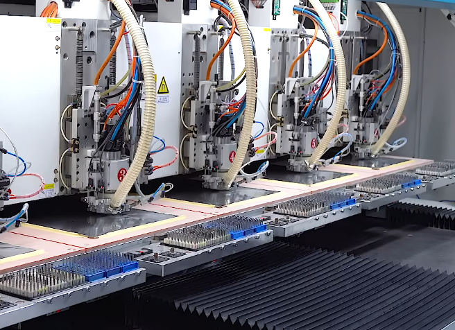
From flight control computers and millimeter-wave radar to high-definition video transmission modules and high-power electronic speed controllers (ESCs), these multilayer PCBs must facilitate complex power distribution, high-speed signal transmission, and precise RF matching—all within an extremely limited footprint.
This article provides an expert perspective, offering an in-depth analysis of the core technologies, manufacturing challenges, and quality standards involved in the production and assembly of multilayer PCBs for drones.
I. Core Technical Requirements and Design Challenges for Multilayer Drone PCBs
Drones feature highly integrated internal spaces and strict weight limitations, while also being subjected to intense mechanical stress and complex electromagnetic interference. These factors impose rigorous technical requirements on the design and manufacturing of their multilayer PCBs.
High-Density Interconnect (HDI) and Micro-via Technology
Modern drone flight control systems typically integrate multi-sensor fusion units (such as IMUs, GPS, compasses, and barometers) alongside high-performance processors. To accommodate hundreds or even thousands of pins within a confined space, multilayer PCBs extensively utilize High-Density Interconnect (HDI) technology.
Blind and Buried Vias: Through the use of laser direct drilling, micro-vias (with diameters of less than 0.1mm) are created—including blind and buried vias—to establish precise electrical interconnections between layers, significantly shortening signal paths.
Stacked and Staggered Via Structures: In complex multilayer PCBs, the strategic design of stacked and staggered vias ensures efficient vertical signal transmission while maintaining the mechanical integrity of specific board sections.
Signal Integrity (SI) and Power Integrity (PI) Management
During high-speed flight, a drone’s video transmission system and digital communication links generate a significant volume of high-frequency digital signals.
Crosstalk and Reflection Suppression: Multilayer boards require careful planning of ground and power planes. By utilizing microstrip and stripline structures, designers can ensure impedance matching for high-speed differential signals (such as MIPI, PCIe, and USB 3.0).
Low-Noise Power Distribution Network (PDN): By strategically placing decoupling capacitors between power and ground planes—and optimizing plane segmentation—the power impedance can be reduced. This prevents system malfunctions or crashes caused by high-frequency switching noise.
Impedance Control and Material Selection
Given that drones often operate in environments with extreme temperature fluctuations and high humidity, the electrical and thermal properties of the substrate materials are critical.
High-Frequency, Low-Loss Materials: For RF and microwave circuits—such as 2.4GHz/5.8GHz video transmission systems or millimeter-wave obstacle-avoidance radar—designers typically use high-frequency materials (e.g., the Rogers series) or specialized PTFE composites to minimize the dielectric constant (Dₖ) and dissipation factor (Df).
High-Tg and Low-CTE Substrates: The primary multilayer boards often utilize FR-4 materials with a high glass transition temperature (High Tg ≥ 170°C). This ensures excellent dimensional stability during high-temperature soldering or sustained high-power operation, preventing via-barrel cracking caused by an excessive coefficient of thermal expansion (CTE) along the Z-axis.
Thermal Design and Heat Management
High-power Electronic Speed Controllers (ESCs), motor driver chips, and high-performance main control processors generate substantial amounts of heat during operation.
Thick Copper Layers and Embedded Copper Blocks: Incorporating 2oz to 4oz thick copper layers within the inner layers of a multi-layer PCB to facilitate large-area heat conduction.
Thermal Via Arrays: Positioning a dense matrix of thermal vias beneath the pads of heat-generating components to rapidly conduct heat to the copper foil or aluminum-based heat sink on the opposite side, ensuring thermal equilibrium within the system.
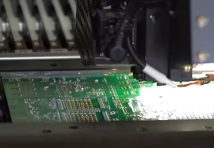
II. Advanced Manufacturing Process for Multi-layer PCBs in Drones
Transforming precise design schematics into high-quality physical multi-layer boards requires dozens of rigorous chemical and mechanical processing steps.
Inner-layer Circuit Pattern Transfer and Precision Etching
The manufacturing of multi-layer boards begins with the inner-layer core.
Laser Direct Imaging (LDI): Utilizing LDI technology instead of traditional exposure equipment achieves micron-level alignment accuracy, completely eliminating registration errors caused by film distortion.
Black/Brown Oxide Treatment: Subjecting the surface of the inner-layer copper foil to micro-etching and chemical conversion creates a uniform organometallic oxide film. This enhances the bonding strength between the inner copper surface and the prepreg, preventing delamination after lamination.
Multi-layer Lamination and Resin Via-Plugging Technology
As the number of layers increases, the complexity of controlling the lamination process rises exponentially.
Vacuum High-Pressure Lamination: In a dust-free environment with constant temperature and high pressure, a precision alignment system is used to thermally bond the inner-layer boards, prepregs, and outer copper foils into a single, integrated structure.
Resin Via-Plugging and Via-Filling: For “via-in-pad” structures in HDI (High-Density Interconnect) boards, non-conductive or conductive epoxy resin is used to plug the vias under vacuum conditions. The surface is then ground flat, allowing components such as BGAs (Ball Grid Arrays) to be mounted directly over the plugged vias.
Laser Drilling and High-Aspect-Ratio Plating
Hybrid UV and CO2 Laser Drilling: Precisely ablating the resin and copper layers to create micro-vias with a high aspect ratio.
Pulse Plating and Copper Thickness Uniformity Control: For high-aspect-ratio through-holes, Pulse Periodic Reverse (PPR) plating technology is employed to ensure a uniform copper layer on the hole walls (typically requiring an average thickness of 20μm or more). This prevents potential cracking caused by an insufficient copper layer within the holes.
Selection and Protection of Surface Finish Processes
The most appropriate surface finish must be selected based on the specific application scenario of the drone PCB:
Electroless Nickel Immersion Gold (ENIG): Offers exceptional surface flatness, making it ideal for soldering fine-pitch BGA components and miniature parts. It also provides strong oxidation resistance, making it the preferred choice for high-end drone flight control boards.
Organic Solderability Preservative (OSP): Cost-effective with a highly flat surface, it is well-suited for lead-free soldering. However, when subjected to multi-zone reflow soldering, careful control of its oxidation resistance and thermal stability is required.
Immersion Silver/Immersion Tin: Often used for specific RF antenna areas, these finishes provide excellent high-frequency signal transmission characteristics.
III. Drone PCB Assembly (PCBA) and High-Reliability Soldering Techniques
The assembly stage, which follows the fabrication of the circuit board, directly determines the quality of electrical connections and the long-term reliability of the entire board.
High-Precision Surface Mount Technology (SMT) for Miniature Components
Drone circuit boards are densely populated with components such as 01005-sized micro-resistors and capacitors, fine-pitch QFNs, WLCSPs, and multi-pin BGA chips.
High-Precision 3D Solder Paste Inspection (SPI): During the printing phase, this technology monitors the thickness, volume, and area of the solder paste in real-time, ensuring that the precise amount of solder is applied to every tiny pad.
High-Speed, High-Precision Pick-and-Place Machines: Integrated with vision recognition systems, these machines enable micron-level component placement, preventing issues such as misalignment, “tombstoning,” or bridging. 2. Optimized Process Control for Reflow and Vapor-Phase Soldering
Multi-Zone Nitrogen-Protected Reflow Soldering: Utilizing a reflow oven with at least 10 heating zones and a high-purity nitrogen atmosphere (O₂ < 50 ppm) reduces solder oxidation, significantly enhancing the wetting properties and mechanical strength of alloy solder joints.
Customized Temperature Profiles: Tailored settings for preheating, soaking, reflow, and cooling zones—adjusted for the specific density of multi-layer boards—prevent thermal shock that could otherwise lead to excessive voiding within BGA components.
Conformal Coating for Harsh Environments
Drones frequently operate outdoors, where they are exposed to rain, high-altitude condensation, salt spray, and dust contamination.
Selective Conformal Coating: Automated selective coating equipment is used to precisely apply polyurethane (UR) or silicone (SR) coatings to the PCB surface, while carefully avoiding sensitive areas such as connectors and optoelectronic sensors.
UV Curing and Coating Thickness Inspection: UV fluorescence inspection ensures complete coverage without air bubbles, creating a robust insulating protective layer that effectively prevents electrochemical migration (such as dendritic growth or CAF failures).
Rigorous End-to-End Quality Inspection and Non-Destructive Testing
Automated Optical Inspection (AOI) and 3D X-Ray: AOI is employed to detect missing, misplaced, or polarity-reversed surface-mount components. 3D X-Ray inspection serves as the final safeguard, ensuring that hidden solder joints—such as those under BGA and QFN packages—are free from voids or cold (defective) solder joints.
In-Circuit Testing (ICT) and Functional Testing (FCT): ICT (using a bed-of-nails fixture) checks for electrical shorts and opens, while customized FCT simulates the drone’s actual operating conditions, performing comprehensive closed-loop functional testing of flight controllers, video transmission systems, and power interfaces.
IV. Quality Verification and Testing Standards for Multilayer PCBs for Drones in Harsh Environments
To ensure that every multilayer PCB delivered for use in drones can withstand the rigorous demands of extreme environments, a stringent reliability verification process must be implemented.
| Test Item | Test Conditions & Methods | Purpose & Evaluation Criteria |
| Dynamic Vibration Test | Complies with MIL-STD-810G standard; performs random and sinusoidal vibration sweeps (frequency: 20Hz – 2000Hz). | Simulates high-frequency vibrations from engines and propellers to verify that solder joints and multi-layer board structures are free from fatigue cracking. |
| Mechanical Shock Test | Half-sine shock pulse (peak acceleration: 50g, pulse duration: 11ms). | Evaluates the shear resistance of the PCB and heavy-duty components during drone takeoff, landing shocks, or hard landings. |
| Thermal Cycling Test | -40°C to +85°C (or higher industrial standards), temperature change rate of 10°C/min, over 500 cycles. | Detects stress tolerance at the interfaces of materials with differing coefficients of thermal expansion (CTE) to prevent barrel cracking or delamination. |
| Temperature-Humidity-Bias (THB) Test | 85°C / 85% RH with bias applied for 1,000 continuous hours. | Verifies the insulation substrate’s resistance to conductive anodic filament (CAF) growth in high-humidity environments to prevent leakage. |
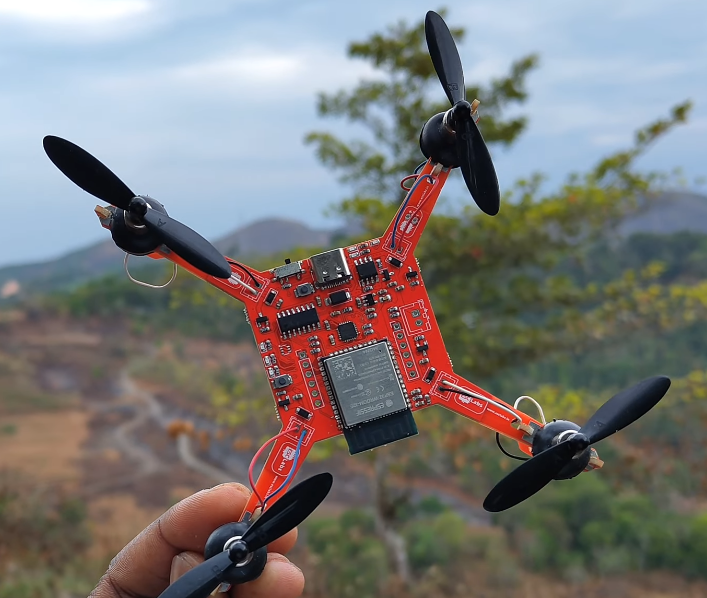
V. Summary and Industry Outlook
The manufacturing and assembly of multi-layer PCBs for drones represent a sophisticated, high-end technological field that integrates materials science, microelectronics engineering, precision mechanics, and chemical engineering.
As drones evolve toward greater autonomous flight capabilities, higher-density payload integration, broader wireless communication frequency bands, and extended operational endurance, the PCB industry faces unprecedented pressure for technological iteration and advancement.
From ultra-thin, high-layer-count HDI (High-Density Interconnect) boards to the integration of embedded passive and active components, the meticulous refinement of every manufacturing step serves as the cornerstone for ensuring that drones fly safely, stably, and efficiently in the skies.
In this wave of technological advancement—driven by the pursuit of extreme reliability and miniaturization—it is critical to partner with a manufacturing service provider that possesses deep technical expertise, cutting-edge production equipment, and a rigorous quality control system.
As a global leader in high-end electronic manufacturing services, KingTop Technology specializes in providing high-precision multi-layer PCB fabrication, complex PCB assembly, and comprehensive, one-stop hardware solutions to clients worldwide.
Leveraging advanced HDI manufacturing processes, precise impedance control, state-of-the-art cleanroom SMT production lines, and stringent aerospace-grade quality inspection standards, KingTop Technology empowers the world’s top drone manufacturers. We transform innovative concepts into rock-solid, high-performance flight-ready realities, helping the industry soar toward an even broader future.