
The onboard electronic architecture of modern Unmanned Aerial Vehicles (UAVs) is undergoing an unprecedented structural transformation.
From consumer-grade aerial photography drones equipped with high-definition gimbals to industrial-grade, heavy-duty UAVs tasked with complex operations—such as surveying and mapping, agricultural crop protection, long-range logistics, and security patrols—the core control systems, high-definition video transmission modules, multi-sensor fusion arrays, and high-power electronic speed controllers (ESCs) are pushing the limits of space and weight allocation.
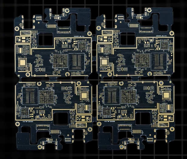
Guided by the core design principle of “Size, Weight, Power, and Cost” (SWaP-C), High-Density Interconnect (HDI) printed circuit board (PCB) technology and microvia fabrication processes have become the cornerstone for building lightweight, high-computing-power, and highly reliable electronic hubs for modern UAVs.
This article examines the architectural evolution of UAV electronic systems, provides an in-depth analysis of core HDI PCB microvia technologies and the challenges of advanced assembly, discusses quality control and testing verification in demanding environments, and explores future technological trajectories.
I. The Evolution of UAV Electronic Systems and the Pivotal Role of HDI PCBs
Analysis of Trends Toward Lightweight Design and High Integration in UAVs
(1) The Dual Evolution of Consumer-Grade and Industrial-Grade UAVs: Consumer-grade UAVs prioritize extreme portability and lightweight design, where foldable airframes and constrained internal compartments impose rigorous limits on the volume and weight of PCBs. Industrial-grade UAVs, meanwhile, require the integration of multispectral cameras, LiDAR, high-precision RTK positioning modules, millimeter-wave radar for obstacle avoidance, and high-power digital video transmission systems—resulting in an unprecedented level of integration density for onboard electronic equipment.
(2) The Extreme Challenge of Load Constraints and Space Compression: Traditional Multi-Layer Boards (MLBs) are no longer sufficient to meet the integration requirements of modern drone flight control systems, obstacle-avoidance sensor arrays, and power management modules, due to restricted routing channels and the significant space consumed by interlayer transitions. With their ultra-high routing density and smaller via dimensions, HDI (High-Density Interconnect) PCBs serve as the essential solution to this conflict.
Performance Comparison: Traditional PCBs vs. HDI PCBs in Drone Applications
(1) Advancements in Line Width and Spacing (L/S): While traditional PCBs typically utilize line widths and spacings of 4 mil/4 mil or greater, HDI PCBs for drones generally employ ultra-fine circuitry—often 3 mil/3 mil or even below 2 mil/2 mil. This drastically improves routing efficiency per unit area, allowing complex digital and analog circuits to coexist within a highly compact footprint.
(2) Lamination Structure and the Advantages of Blind/Buried Vias: By incorporating laser-drilled microvias, HDI boards enable direct interconnection between specific layers. This reduces signal loss, parasitic capacitance, and space wastage—issues commonly associated with traditional through-holes—while significantly shortening the transmission paths for radio frequency (RF) and high-speed digital signals.
High-Standard PCB Requirements for Avionics, Flight Control, and Image Transmission Systems
(1) Flight Control Systems: These require exceptional reliability and resistance to interference. The multi-layer lamination structure of HDI boards provides superior power planes and ground shielding, effectively suppressing electromagnetic interference (EMI) and ensuring the accurate acquisition of data from inertial measurement units (IMUs) and other sensors.
(2) HD Image Transmission and AI-Powered Visual Processing: Involving high-speed differential signals (such as MIPI, PCIe, and USB 3.0), HDI microvia technology effectively minimizes impedance discontinuities. This preserves signal integrity (SI) and ensures the zero-latency transmission of high-definition video streams.
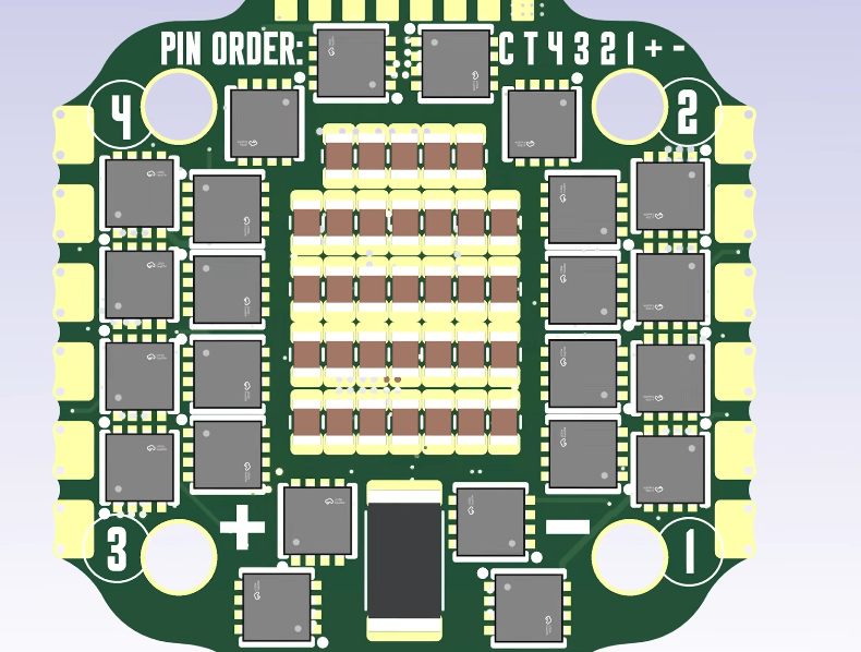
II. Key Technologies for Microvia Processes in Drone HDI PCBs
Microvia Formation Technology (Comparison and Integration of Laser and Mechanical Drilling)
(1) Application of UV and CO2 Lasers: For the resin layers and copper foils commonly found in drone HDI PCBs, a hybrid laser process is typically employed: a UV laser is used to open a “window” in the copper, followed by a CO2 laser to ablate the underlying dielectric material (such as resin or glass-reinforced fabric). This approach enables the creation of microvias with diameters of less than 100μm—or even 50μm—achieving a level of precision far superior to that of traditional mechanical drilling.
(2) Microvia Aspect Ratio Control: To ensure high-quality electroplated via filling, the aspect ratio (the ratio of depth to diameter) must be precisely calculated—typically maintained at or below 1:1 or 0.8:1. This prevents issues such as poor chemical exchange or the formation of voids within the plated via, which can occur if the via is too deep.
Microvia Metallization and Electroplated Via Filling (Via-in-Pad and Blind/Buried Via Technologies)
(1) Via-in-Pad (VIPPO) Technology: This technique allows microvias to be placed directly within component pads, significantly saving surface area. It is particularly well-suited for areas on a drone’s main control board—such as those housing dense BGA (Ball Grid Array) chips—by effectively addressing the challenges of routing traces in high-density packaging.
(2) Electroless and Electroplated Copper Filling: By utilizing specialized additives (such as leveling agents and brighteners) in conjunction with pulse or DC electroplating, microvias can be completely filled. This ensures a flat pad surface, which is essential for the reliability and planarity of subsequent SMT (Surface Mount Technology) component soldering. Microvia Reliability and Thermomechanical Stress Management
(1) Coefficient of Thermal Expansion (CTE) Matching: During flight, drones experience drastic temperature fluctuations—transitioning from high-temperature, high-humidity conditions on the ground to the extreme cold of high altitudes. The Z-axis CTE of the PCB substrate (such as high-Tg FR-4 or PTFE materials) must be strictly matched with that of the copper used to fill the vias. This prevents thermal stress from causing microvia fractures or interlayer delamination.
(2) Interconnect Stress Testing (IST) and Thermal Shock Validation: Through rigorous thermal cycling tests, the fatigue life of microvias during long-term service is evaluated, ensuring that electrical connections remain robust even under extreme temperature differentials.
III. Advanced Manufacturing and Assembly Processes for Drone HDI PCBs
Challenges in High-Density Component Placement and Surface Mount Technology (SMT)
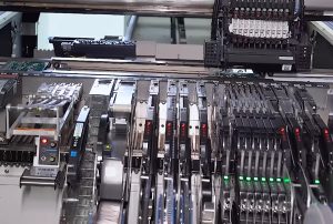
(1) Precision Challenges with Miniature Components: Drone motherboards frequently utilize ultra-miniature passive components (such as 01005 and 0201-sized resistors and capacitors) as well as fine-pitch QFN, BGA, and CSP chips. These components demand exceptional placement accuracy, high-precision vision recognition systems, and highly stable component feeders.
(2) Stencil Design and Solder Paste Printing Optimization: The use of nano-coated stencils and laser-cutting technology allows for precise control over solder paste deposition. This helps prevent defects such as solder beads, bridging, or insufficient solder, ensuring that tiny pads receive an adequate volume of solder paste.
Soldering and Reflow Optimization for Fine-Pitch Components
(1) Reflow Profile Customization: Due to the high layer count and uneven copper thickness of HDI boards, the distribution of thermal capacity is complex. Reflow oven temperature zones must be optimized to account for the differing heat-absorption characteristics of large power components versus miniature chips, ensuring uniform temperature distribution across the entire PCB surface.
(2) Nitrogen-Shielded Soldering: Introducing a nitrogen atmosphere during the soldering of critical RF modules and multi-layer HDI (High-Density Interconnect) boards reduces surface tension, significantly improves solder joint wettability and luster, and enhances oxidation resistance.
Conformal Coating & Potting for Complex Environments
(1) Protection Against Moisture, Dust, and Salt Spray: Since drones frequently operate in complex outdoor climates, assembled PCBAs must be treated with a conformal coating (such as acrylic, silicone, or polyurethane). Additionally, critical interfaces should be secured via dispensing or localized potting to prevent moisture ingress, which could otherwise cause short circuits.
(2) Coating Process Control: It is essential to ensure that areas with micro-vias and high-voltage pads remain free of bubbles, pinholes, or excessive coating thickness—the latter of which can lead to concentrated mechanical stress—while balancing the need for electrical insulation with effective heat dissipation.
IV. Quality Control, Testing, and Reliability Verification
RF Performance Testing and Impedance Control
(1) Strict Impedance Control: As drone video transmission and remote control links operate in the 2.4 GHz, 5.8 GHz, or even higher frequency bands, the dielectric constant (Dk) and trace-width tolerances of HDI boards must be maintained within ±5% to ensure efficient RF energy transmission.
(2) Vector Network Analyzer (VNA) Testing: S-parameter testing is performed on antenna feed lines and RF front-end circuits to optimize return loss and insertion loss, thereby preventing communication interruptions caused by signal reflection.
Environmental Adaptability Testing (Vibration, Temperature Extremes, and Low-Pressure/High-Altitude Conditions)
(1) Mechanical Vibration Simulation: The high-speed rotation of drone motors generates continuous, high-frequency vibration. Assembled HDI boards must undergo random vibration testing to verify the fatigue resistance of solder joints and micro-vias, ensuring that resonance does not lead to solder joint cracking.
(2) High-Altitude, Low-Pressure Environment Verification: Simulates the insulation performance of electrical clearances under low-pressure conditions typical of high altitudes. This prevents corona discharge or electrical breakdown between microvias, ensuring operational safety at high altitudes.
Application of Non-Destructive Testing (NDT) Technologies (X-ray, AOI, 3D SPI) in Assembly
(1) 3D SPI (Solder Paste Inspection) and AOI (Automated Optical Inspection): These technologies are employed during the initial printing and component placement stages to detect defects—such as misalignment, insufficient solder, or excess solder—in real time, allowing for quality control at the very source of production.
(2) High-Resolution Micro-focus X-ray Inspection: Specifically used to examine the internal structure of BGA packages, including the voiding ratio of solder balls and the plating quality within microvias and blind vias, ensuring that hidden internal defects are identified.
Conclusion
In summary, the assembly and microvia processing of HDI PCBs for drones represent a highly complex, multidisciplinary, and advanced manufacturing technology. From micron-level laser drilling and precise electroplated via-filling to high-density surface mounting and rigorous environmental reliability testing, every step is critical to ensuring a drone’s flight safety and mission effectiveness in complex airspace.
As drones evolve toward greater intelligence, autonomous swarming capabilities, and all-weather operational readiness, the requirements for HDI PCB layer counts, circuit density, and microvia reliability will become increasingly demanding.
Amidst this technological evolution, KingTop Technology—a global leader in Electronics Manufacturing Services (EMS) and high-end PCB solutions—leverages its deep technical expertise in microvia processing, high-density assembly, and the manufacturing of RF and high-speed circuit boards. The company provides comprehensive, one-stop services for clients in the drone, aerospace, and smart hardware sectors, spanning PCB prototyping, precision manufacturing, complex PCBA assembly, and end-to-end reliability testing.