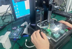
Power supply PCB assembly and SMT (Surface Mount Technology) processing are core components of electronics manufacturing.
Because power supply boards handle high voltages, high currents, and high-frequency switching signals, they impose rigorous requirements regarding placement precision, solder joint reliability, thermal management design, and quality control.
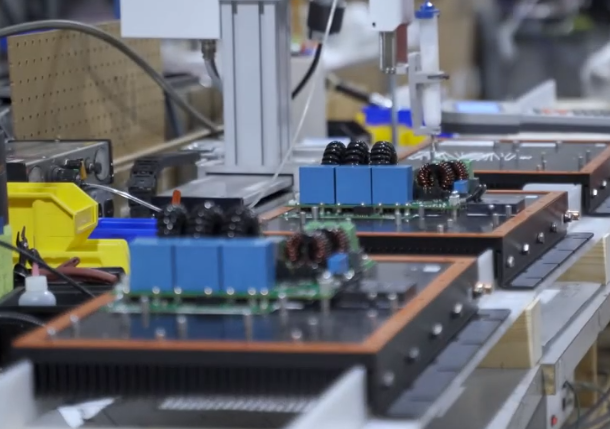
I. Technical Characteristics of Power Supply PCB Assembly and SMT Processing
The manufacturing logic for power supply PCBA differs significantly from that of standard consumer electronics. Power supply products typically incorporate power components (MOSFETs, IGBTs), bulky inductors, high-voltage capacitors, and precision control ICs; the overall manufacturing process is characterized by a combination of high component density and high power output.
Requirements for High-Density and Thick-Copper Board Processing
Power supply PCBs often utilize designs with copper weights of 2 oz or greater; some multilayer boards feature copper thicknesses reaching 4 oz to 6 oz. Thick-copper boards absorb substantial heat during SMT printing and reflow soldering, which can easily lead to cold solder joints or “false” (incomplete) joints. Consequently, precise calibration of the reflow temperature profile is critical to ensuring soldering quality.
Placement Challenges for Odd-Form and Bulky Components
Power supply boards feature numerous power components and large-package devices (such as TO-220, D2PAK, and PQFN), requiring precise control of placement pressure and nozzle selection. Heavy components are prone to shifting during the reflow process due to uneven surface tension; auxiliary measures such as the “Red Glue Process” (adhesive bonding) or selective soldering are often required.
Balancing Soldering with Heat Conduction and Thermal Copper Pours
Power supply circuit designs typically include large areas of copper for grounding and heat dissipation. During SMT soldering, these thermal copper pours can rapidly dissipate heat, creating a “thermal sink” effect that prevents solder pads from reaching the required temperature. Manufacturing processes must optimize pad connections through DFM (Design for Manufacturability)—such as using thermal relief pads—and appropriately adjust the reflow profile’s ramp-up rate and soak time.
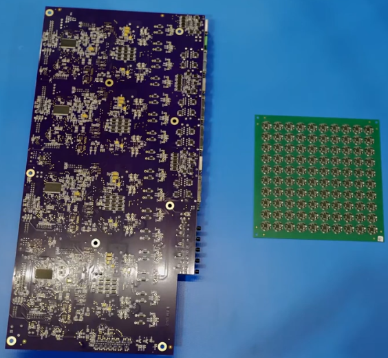
II. Process Specifications for the Complete Power Supply SMT Manufacturing Workflow
Precision control in power supply PCB assembly extends across the entire product lifecycle, from raw material intake to final inspection.
Solder Paste Printing Process Control
Stencil Design: To accommodate the coexistence of components of varying sizes on power boards, step stencils are utilized. Apertures for high-power component pads are appropriately enlarged or designed with grid patterns to minimize voiding, while pads for small-package control chips feature reduced-size designs to prevent bridging.
Thickness and Tension Standards: Stencil tension must be maintained above 35 N/cm to ensure crisp solder paste release edges and prevent solder bridging (short circuits).
High-Precision SMT Placement
Vision System: High-resolution cameras are used for the alignment of power control ICs (e.g., PWM controllers, MCUs) and components in QFN or BGA packages.
Placement Pressure Settings: Precise placement pressure is set for large power components to prevent solder paste collapse and short circuits caused by excessive force, or issues such as “tombstoning” and misalignment resulting from insufficient pressure.
Reflow Soldering and Temperature Profile Optimization
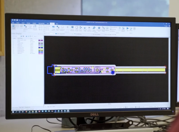
Reflow soldering is the critical stage of power supply assembly; specialized soldering profiles (for 10-zone or 12-zone systems) must be established based on board thickness and thermal mass:
| Reflow Phase | Temperature Range | Duration | Process Control Key Points |
| Preheat Zone | 120°C – 160°C | 60 – 100 s | Slow temperature rise to prevent PCB deformation caused by excessive thermal gradient |
| Soaking Zone | 150°C – 200°C | 60 – 120 s | Fully activate flux and reduce thermal imbalance on heavy copper boards |
| Reflow Zone | Peak 235°C – 250°C | 40 – 70 s (Above Liquidus) | Ensure complete melting of power device pads and keep voiding rate below 10% |
| Cooling Zone | Cooling Rate 3 – 5 °C/s | – | Fast cooling to form fine grain structure and improve solder joint mechanical strength |
DIP Assembly and Selective Soldering (THT & Selective Soldering)
Components such as transformers, large capacitors, and terminal blocks on power supply boards are typically Through-Hole Technology (THT) components. Modern power supply manufacturing facilities commonly employ selective wave soldering or selective dip soldering processes to precisely solder THT leads, thereby avoiding the thermal shock that traditional full-board wave soldering imposes on Surface Mount Technology (SMT) components.
III. Quality Inspection and Reliability Assurance for Power Supply PCB Assembly
Power supply products operate under conditions of high voltage, high current, and significant heat generation over extended periods; consequently, stringent requirements are placed on non-destructive testing and electrical reliability.
3D SPI and 3D AOI Inspection
SPI (Solder Paste Inspection): Performs 100% 3D scanning of solder paste volume, area, thickness, and offset prior to component placement, catching printing defects before the SMT stage.
AOI (Automated Optical Inspection): Conducts comprehensive inspections after component placement and reflow soldering to accurately identify incorrect components, missing components, reversed polarity, cold solder joints, and solder bridging.
X-Ray Non-Destructive Testing
The thermal pads (base pads) of power devices (such as DFN, QFN, and BGA packages) play a critical role in heat dissipation. X-ray inspection allows for the direct measurement of the soldering voiding rate at these thermal pads. Soldering standards for power supplies typically require the voiding rate of critical thermal pads to remain below 10%–15% to prevent heat accumulation that could lead to device breakdown.
Conformal Coating Process
PCBAs for industrial power supplies, new energy vehicle power systems, and outdoor power units require automated conformal coating (providing protection against moisture, salt spray, and mold). Selective coating equipment is used to protect high-voltage areas and dense IC pin arrays while strictly avoiding connectors, switches, and test points.
IV. Common Defects and Solutions for Power Supply PCBA
The following are common engineering issues and corresponding countermeasures encountered during the assembly and SMT production of power supply PCBs:
Excessive voiding under power components
Cause: Large pad areas prevent flux volatiles from escaping in time during solder paste reflow.
Countermeasures: Optimize the stencil aperture design by switching to a grid-like (Matrix/Window pane) pattern; adjust the soak zone duration in the reflow profile to ensure complete flux volatilization; implement a vacuum reflow process if necessary.
Creepage and breakdown in high-voltage areas
Cause: Residual flux (which absorbs moisture) or solder spatter remaining on the board surface after SMT placement compromises the creepage distance, causing it to fall short of safety standards.
Countermeasures: Utilize high-insulation-resistance water-wash or no-clean processes and strictly adhere to ultrasonic or water-washing procedures; ensure that spacing in high-voltage areas complies with GB/IEC safety standards.
Tombstoning and skewing of odd-form transformers/inductors
Cause: Uneven thermal capacity between pads at either end leads to unbalanced molten solder surface tension; alternatively, the SMT placement machine nozzle selection is inappropriate.
Countermeasures: Balance the thermal design of copper pours on the pads at both ends; use custom-made, non-standard nozzles; optimize the placement machine’s acceleration and placement force.
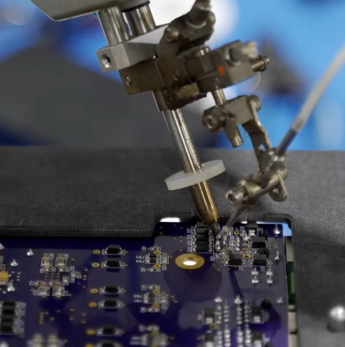
V. Manufacturing Process Flowchart and Quality Control Summary
To ensure the delivery of highly reliable power supply PCB assemblies, the entire production chain strictly adheres to the following standardized manufacturing workflow:
- (1) Material requisition and baking (to prevent cracking)
- (2) 3D SPI (Solder Paste Inspection)
- (3) SMT high-speed/multi-function component placement
- (4) 10/12-zone reflow soldering
- (5) X-ray and 3D AOI (Automated Optical Inspection)
- (6) DIP (Through-hole) insertion and selective wave soldering
- (7) Functional Testing (FCT) and Burn-in testing
- (8) Conformal coating and finished product packaging
Through meticulous end-to-end management—encompassing DFM (Design for Manufacturability) assessment, stepped stencil design, vacuum/multi-zone reflow soldering, and X-ray void inspection—product yield and long-term reliability for power supply PCB assemblies and SMT processing are significantly enhanced.
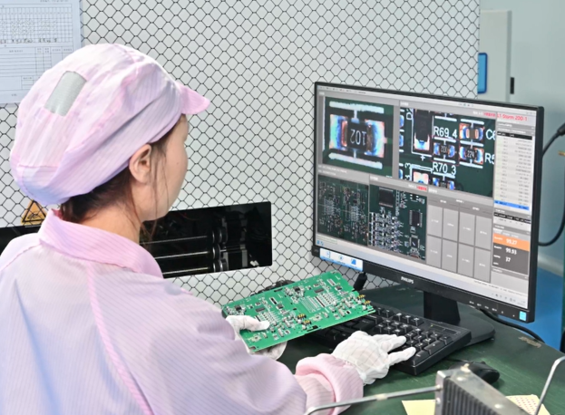
Summary
Power supply PCB assembly and SMT processing constitute far more than a simple assembly procedure; they represent a comprehensive engineering process involving thermodynamic balance, electrical insulation, high-power soldering, and high-reliability inspection.
From upfront Design for Manufacturability (DFM) assessments and optimized stepped-stencil designs to the precise control of multi-zone or vacuum reflow soldering, and through to 100% X-ray void inspection and conformal coating protection, every step directly determines the lifespan and safety of the final power supply product. Only through the rigorous implementation of standardized quality control across the entire process can the power supply PCBA ensure long-lasting, stable, and efficient operation under conditions of high voltage, high current, and harsh environments.