
Microcontroller Development Board Solution Provider: Hardware Design and Engineering Implementation for Custom Development Boards.
A microcontroller (MCU) development board is more than just an MCU chip mounted on a PCB. For industrial control systems, smart instruments, IoT terminals, and embedded devices, a development board must balance processor performance, peripheral circuitry, communication interfaces, power management, and system stability—all within a constrained space.
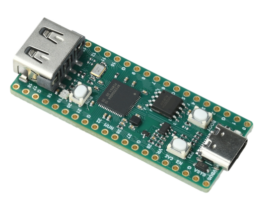
Because different applications have vastly different requirements regarding real-time response, power consumption, the number of interfaces, and operating environments, off-the-shelf development boards often fall short of specific product needs.
The core of a custom microcontroller development board lies in re-architecting the hardware to create a cohesive system solution where the MCU, peripheral circuits, and the intended application are perfectly aligned.
Defining the MCU Architecture Based on Application Requirements
The first step in developing a custom board is not selecting a specific chip, but rather defining the tasks the control system must perform.
For instance, industrial control equipment typically prioritizes real-time response, ADC sampling precision, PWM output, and noise immunity. Smart sensors require low-power operation, multi-channel data acquisition, and stable wireless communication. Consumer electronics, meanwhile, often emphasize compact size, cost-effectiveness, and high peripheral integration.
During the design phase, key parameters to evaluate include:
Processing Performance: Determine the MCU’s core architecture, clock frequency, and memory resources based on control algorithms, data processing volume, and real-time task requirements.
Memory Configuration: Assess the necessary Flash and SRAM capacity; incorporate external memory if needed to support data caching, logging, or firmware updates.
Peripheral Resources: Configure GPIO, ADC, DAC, PWM, timers, and interrupt resources according to specific operational needs.
Communication Capabilities: Select appropriate interfaces—such as UART, SPI, I²C, CAN, USB, or Ethernet—and integrate wireless modules (e.g., Wi-Fi or Bluetooth) when required.
MCU families from manufacturers like STMicroelectronics (STM32), NXP, Microchip, and Renesas offer varying resource configurations and are tailored for different applications.
The final selection should be based on a holistic assessment of functional requirements, supply lead times, product lifecycle, and total Bill of Materials (BOM) cost, rather than simply chasing the highest possible processing performance.
Key Hardware Design Considerations for Custom Development Boards
The stability of a microcontroller (MCU) development board depends largely on the design of its peripheral circuitry. Even if the MCU itself is highly capable, issues such as excessive power supply ripple, clock irregularities, or a poorly designed reset circuit can lead to system instability.
Power Management and Voltage Regulation
Different MCUs and peripheral components may require varying operating voltages. The design process must account for DC-DC converters, LDO regulators, power filtering, and power-up sequencing, with careful calculation of power margins based on load variations. For boards that include motor drivers, relays, or wireless transmission modules, it is also essential to ensure that the switching of high-current loads does not interfere with the core control circuitry.
Clock and Reset Circuits
External crystal oscillators, load capacitors, and their associated PCB traces must be matched according to the chip manufacturer’s reference design. For applications involving USB, CAN, or other protocols that demand high clock precision, particular attention must be paid to clock error and stability. The reset circuit must ensure that the MCU can start up reliably or recover properly during power-on, power-off, or unexpected voltage fluctuations.
Interfaces and Peripheral Circuitry
Custom development boards often require specific expansion interfaces tailored to the overall system functionality. For instance, industrial equipment might require isolated RS485, CAN, or digital I/O; sensor-based devices may need high-precision ADCs, analog front-ends, and low-noise power supplies; while smart terminals might incorporate displays, memory card slots, and wireless communication modules.
Interface design goes beyond simple physical connectivity; it must also address voltage-level compatibility, drive strength, ESD protection, and safeguards against reverse-connection.
PCB Layout and Routing: The Foundation of Stable Operation
A correct schematic does not guarantee a reliable physical PCB. For microcontroller development boards, the PCB layout must carefully manage the interactions between digital signals, analog signals, power loops, and high-speed interfaces.
Key design aspects include:
Power Integrity: Place appropriate decoupling capacitors near the MCU’s power pins, shorten power return paths, and minimize transient voltage fluctuations.
Analog and Digital Domains: Strategically position ADC inputs and analog front-ends for sensors away from digital switching circuits to reduce noise coupling.
High-speed signals: For interfaces such as USB and Ethernet, control impedance, trace length, and reference plane continuity in accordance with specific standards.
Grounding design: Plan for a continuous reference ground plane, with a focus on managing return paths for switching power supplies, high-current loads, and sensitive analog signals.
EMC and ESD: Implement appropriate protective measures at external interfaces, power entry points, and locations susceptible to electrostatic discharge.
If the development board is intended for installation within a compact device, factors such as board dimensions, connector height, mounting hole placement, thermal management space, and assembly methods must be considered concurrently. This prevents structural constraints from necessitating redesigns after the circuit layout is finalized.
Firmware Debugging and Hardware Functional Verification
The development of a custom board should not end at the PCB prototyping stage. Once the hardware design is complete, firmware debugging is required to verify that the chip’s resources align with the actual circuit implementation.
Typical development and debugging tasks include:
Configuring debugging interfaces supported by the chip, such as SWD or JTAG.
Verifying boot modes, startup circuitry, and firmware download paths.
Testing peripheral functions, including GPIO, ADC, PWM, UART, SPI, and I²C.
Validating watchdog timers, exception-triggered resets, low-power modes, and wake-up mechanisms.
Testing communication stability, sensor sampling accuracy, and peripheral compatibility.
For products requiring remote maintenance, the hardware architecture should include provisions for firmware updates. Depending on the application, this may involve designing a bootloader, a dual-partition update system, or a rollback mechanism in the event of an update failure.
This step is valuable for identifying hardware-software compatibility issues early, thereby reducing the risk of having to repeatedly modify the PCB during the full-system development phase.
Transitioning from Engineering Prototypes to Mass Production
A functional prototype does not necessarily mean a design is ready for mass production. The engineering verification phase must also address component substitution, soldering processes, test coverage, and long-term supply chain stability.
For PCBA manufacturing, the appropriate assembly process—SMT, DIP, or a hybrid approach—must be selected based on the board’s structure, with careful inspection of solder quality for packages such as QFN and BGA.
For critical control boards, a comprehensive testing strategy—incorporating methods like SPI, AOI, X-ray inspection, ICT, and functional testing—should be established, tailored to the specific risk profile of the product. Furthermore, the design phase should account for the inclusion of test points, programming/download interfaces, production-grade firmware flashing methods, and product serial number management.
For devices requiring ongoing iteration, establishing a clear mapping between BOM versions, PCB revisions, and firmware versions is essential for long-term maintenance and efficient mass production management.
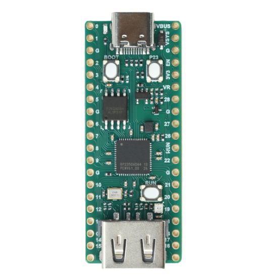
KingTop Technology: Custom Microcontroller Development Board Solutions and PCBA Manufacturing Support
Specializing in PCB fabrication and PCB assembly, KingTop Technology provides comprehensive engineering support—from PCB design and manufacturing to final circuit board assembly—tailored to the specific requirements of a client’s embedded electronic products.
For microcontroller development board projects, KingTop Technology offers end-to-end services, including PCB engineering design, component procurement, SMT placement, soldering/assembly, and rigorous testing—all aligned with the product’s functional requirements, physical dimensions, interface configurations, and production specifications.
For projects transitioning from prototype validation to mass production, we also optimize PCB architecture and PCBA design for manufacturability (DFM), ensuring the board is well-suited for large-scale production and testing.
A microcontroller development board truly ready for product deployment does more than just get the MCU running; it ensures the entire circuit system remains stable in real-world operating environments, while also being testable, manufacturable, and capable of supporting future iterations. This is the key distinction between a custom development board solution and standard circuit board fabrication.