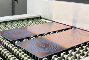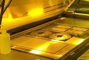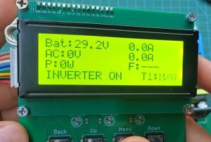

A solar inverter does more than simply convert direct current (DC) into alternating current (AC). The entire conversion process involves high-frequency switching, power device driving, voltage sampling, current feedback, and complex protection and control mechanisms.
In the context of PCB and PCBA manufacturing, the true challenge lies not merely in accurately soldering components onto a circuit board, but in ensuring that the circuitry remains stable under conditions of high voltage, high current, and sustained temperature rise.
Solar inverter PCB assembly requires the seamless integration of electrical design, PCB fabrication, and electronic assembly. Any process deviation at any stage can compromise the conversion efficiency and operational reliability of the entire unit.
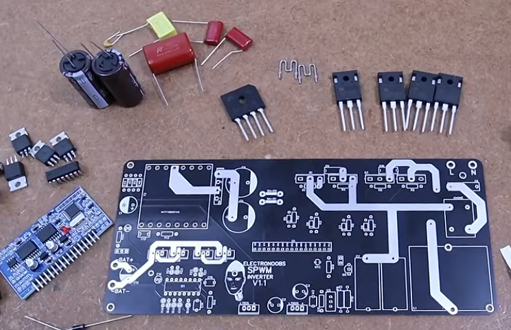
Inverter PCB Manufacturing: Starting with the Power Path
A solar inverter typically comprises a DC input, MPPT (Maximum Power Point Tracking) control, a DC bus, power switching bridge arms, drive circuitry, and auxiliary control modules. Each section imposes distinct requirements on the PCB.
Power Circuitry Area: The primary focus here is high-current carrying capacity. Design considerations must account for operating current, copper thickness, trace width, and temperature rise limits to prevent localized overheating. Furthermore, high-current loops should be kept as compact as possible to minimize parasitic inductance.
Control and Sampling Area: Voltage and current sampling signals are susceptible to noise generated by power switches. PCB layout must carefully manage the separation of analog ground from power return paths, ensuring that high di/dt (rate of change of current) loops do not intersect with sensitive signal areas.
High-Voltage Isolation Area: Between the high-voltage DC side and the low-voltage control side, electrical clearance and creepage distances must be determined based on operating voltage, pollution degree, material properties, and relevant safety standards. Simply increasing the number of PCB layers is not a sufficient solution for achieving proper isolation.
Key Aspects of PCB Assembly: Power Devices and Thermal Management
In the manufacturing of inverter PCBA, components such as MOSFETs, IGBTs, rectifiers, and power inductors are subjected to significant electrical and thermal loads. The quality of their soldering and their physical layout are directly linked to the overall stability of the system. Key areas for control include the following:
Thermal Management during Soldering: Due to the significant difference in thermal capacity between large-sized power components and standard surface-mount devices (SMDs), the reflow soldering temperature profile must be carefully configured to prevent issues such as inadequate soldering or excessive thermal stress.
Thermal Pad Quality: For components with bottom-side thermal pads, attention must be paid to solder paste aperture design, stencil configuration, and the void ratio within the solder joints, as these factors directly impact thermal conductivity.
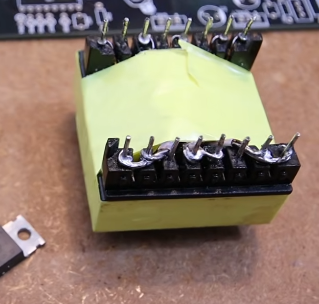
Assembly of Large-Sized Components: For components such as transformers, inductors, connectors, and parts with substantial heat-dissipation structures, factors such as mechanical fixation, the load-bearing capacity of solder joints, and the operating vibration environment must be taken into account.
Mixed Assembly Processes: A combination of SMT (Surface Mount Technology), THT (Through-Hole Technology), and selective soldering processes should be employed based on the product structure to ensure reliable solder connections for all component types.
For high-power inverters, the structural integrity of solder joints is merely the baseline; other critical concerns include solder joint fatigue under long-term thermal cycling, the integrity of thermal conduction paths, and the impact of mechanical stress.
Electromagnetic Compatibility (EMC): Addressing Issues Before Final Product Testing
Inverters utilize high-frequency power switches, where switching nodes generate high rates of voltage change (dv/dt) and current change (di/dt), which can easily lead to conducted and radiated interference.
PCBA design and manufacturing require special attention to:
Isolation between power-switching loops and sensitive control signals.
The length, return paths, and parasitic parameters of gate-drive circuitry.
Control of copper foil area at high-speed switching nodes.
Grounding architecture, shielding connections, and interface filtering design.
Noise immunity for current-sensing and voltage-feedback signals.
These challenges cannot be resolved simply by adding more filtering components. A robust PCB layout, a sound grounding strategy, and consistent assembly processes are the fundamental requirements for mitigating the risk of electromagnetic interference (EMI).
Quality Verification for Solar Inverter PCBAs
Testing protocols for inverter circuit boards should be tailored to the product’s power rating, operating voltage, and application environment. Beyond standard visual inspections, the actual electrical performance must also be rigorously evaluated.
It should be noted that AOI (Automated Optical Inspection) and ICT (In-Circuit Testing) cannot fully replace operational verification of the complete unit. For inverter PCBA (Printed Circuit Board Assembly), tests such as full-load operation, temperature rise assessment, and the verification of protection functions are equally critical; specific test conditions should be determined based on the product’s design requirements.
KingTop Technology: Manufacturing Support for Solar Inverter PCBs and PCBAs
KingTop Technology specializes in PCB fabrication and PCB assembly, providing circuit board manufacturing and electronic assembly services for products in the industrial and power electronics sectors.
For solar inverter projects, KingTop Technology focuses not only on board fabrication and component placement but also on ensuring the alignment between the PCB structure and the assembly process. Through project documentation review, confirmation of component assembly requirements, and rigorous production quality control, we help clients minimize friction between the design and manufacturing phases.
Whether dealing with power control boards or auxiliary driver boards, different PCB modules require specific materials, soldering techniques, and inspection protocols. Based on a client’s Gerber files, Bill of Materials (BOM), and assembly specifications, KingTop Technology provides comprehensive process evaluation and production execution for PCB and PCBA manufacturing projects.
For custom-developed inverters, considering manufacturing feasibility, the supply of critical components, and downstream testing requirements early in the process helps ensure production consistency and mitigates potential risks during the product introduction phase.
Conclusion
The core of solar inverter PCBA manufacturing lies not merely in achieving faster component placement speeds, but in integrating power components, circuit architecture, soldering processes, and thermal management into a reliable, cohesive system.
From the design of the PCB copper traces and the soldering of power components to the verification of electrical performance and temperature rise, every detail influences the final product’s operational behavior. Partnering with a provider that possesses integrated capabilities in both PCB fabrication and PCB assembly is a vital step toward enhancing the manufacturing quality of solar inverters.