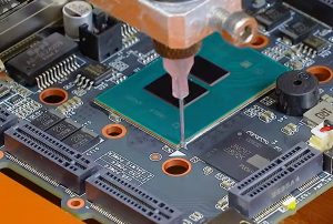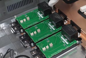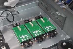

Optical sensors are widely used in industrial automation, smart home systems, medical electronics, consumer electronics, and automotive electronics.
Their primary functions include detecting light intensity, identifying changes in light conditions, and converting optical signals into electrical signals. As electronic devices continue to evolve toward miniaturization, higher precision, and lower power consumption, optical sensor PCB assembly requires increasingly strict control over manufacturing accuracy, soldering quality, and signal stability.
Optical sensor PCB assembly involves more than conventional SMT placement and soldering. It also requires careful attention to optical component positioning, signal circuit layout, environmental interference control, and functional verification.
1. Basic Requirements for Optical Sensor PCB Assembly
Optical sensor circuits typically consist of photosensitive components, signal conditioning circuits, amplifiers, microcontrollers, and power management circuits. Different types of optical sensors have different PCB design and assembly requirements.
The main considerations include:
- Assembly Accuracy: Ensure precise placement of photodiodes, photoresistors, and other sensitive electronic components.
- Soldering Quality: Maintain reliable solder joints and prevent cold solder joints, solder bridging, and component damage.
- Signal Stability: Minimize the impact of power supply noise and electromagnetic interference on weak optical signals.
- Optical Structure: Properly control sensor positioning, orientation, and surrounding shielding structures.
- Long-Term Reliability: Ensure stable operation under temperature variations, vibration, and demanding environmental conditions.
These requirements should be considered throughout PCB design, component sourcing, and manufacturing.
2. Main Processes in Optical Sensor PCB Assembly
Optical sensor PCB assembly typically uses Surface Mount Technology (SMT). Depending on product requirements, additional processes such as Through-Hole Technology (THT), manual soldering, and optical component assembly may also be necessary.
2.1 PCB Manufacturing and Incoming Inspection
Before production begins, the PCB should be inspected for dimensions, layer count, copper thickness, surface finish, and solder pad quality.
For high-precision optical sensor circuits, particular attention should be given to grounding design, signal routing, and power distribution to prevent PCB manufacturing variations from affecting subsequent assembly.
2.2 Solder Paste Printing
An automated stencil printer applies a controlled amount of solder paste to the designated PCB pads.
This process requires precise control over stencil aperture design, solder paste thickness, and printing alignment. Uniform solder paste coverage helps reduce insufficient solder, component misalignment, and solder bridging.
2.3 SMT Component Placement
High-speed pick-and-place machines install photosensitive components, resistors, capacitors, operational amplifiers, control ICs, and other electronic components onto their designated PCB positions.
For components such as photodiodes and photosensitive sensors, which have specific orientation requirements, placement must strictly follow the PCB design and component specifications to prevent polarity errors and installation deviations.
2.4 Reflow Soldering
The PCB passes through a reflow oven, where controlled temperature stages, including preheating, soaking, reflow, and cooling, allow the solder paste to melt and form reliable solder joints.
During production, the temperature profile must be adjusted according to component thermal characteristics and solder paste specifications to prevent excessive thermal stress on temperature-sensitive components.
2.5 Through-Hole and Additional Assembly
Some optical sensor products also include connectors, pin headers, shielding covers, and other through-hole components.
Depending on the product structure, automated insertion or manual-assisted soldering may be used. For products requiring precise optical alignment, additional components such as lenses, light shields, and optical windows must also be properly installed.
3. Quality Inspection for Optical Sensor PCB Assembly
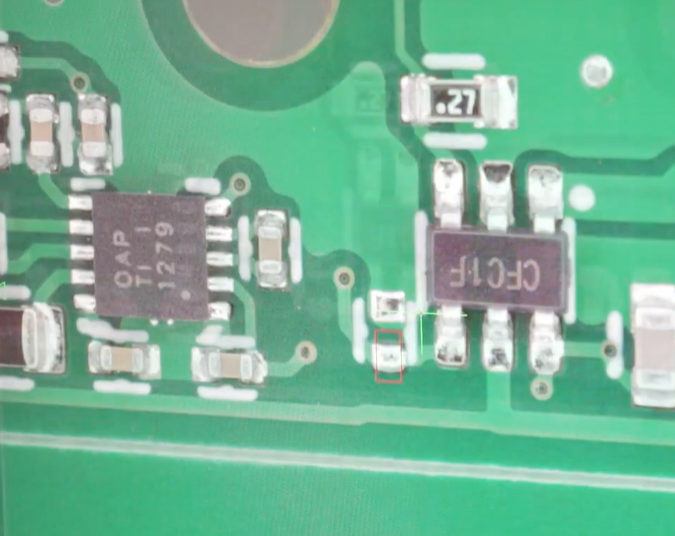
Quality inspection is essential for ensuring the stable operation of optical sensor products. In addition to conventional solder joint inspection, electrical performance testing and optical response verification are also required.
| Inspection Method | Main Inspection Items |
|---|---|
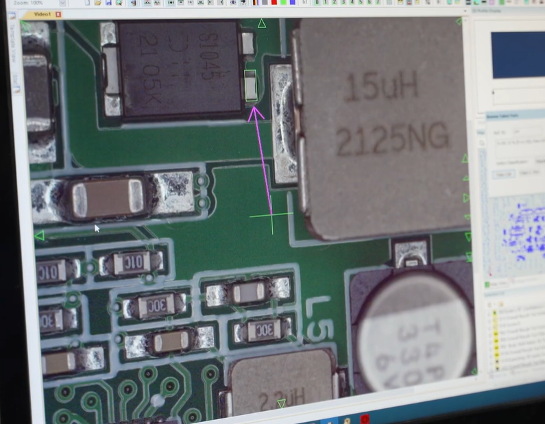
| AOI Inspection | Component misalignment, missing components, and soldering defects |
| X-Ray Inspection | Hidden solder joints in BGA, QFN, and other packages |
| ICT Testing | Circuit connectivity, short circuits, and open circuits |
| FCT Testing | Power supply, communication, and overall functionality |
| Optical Testing | Light response, sensitivity, and detection accuracy |
Optical testing is particularly important. By testing the sensor under different light intensities and environmental conditions, manufacturers can verify whether it accurately detects changes in light and produces signals that meet design specifications.
4. Key Process Control Factors in Optical Sensor PCB Assembly
Compared with conventional control circuits, optical sensor PCBs are more sensitive to certain manufacturing details.
First, control photosensitive component placement. The position and orientation of optical components directly affect light reception. Accurate placement and consistent optical structures are essential.
Second, minimize circuit noise interference. For weak optical signals, proper grounding, power filtering, and signal routing are necessary to reduce external electromagnetic interference.
Third, control soldering temperatures. Some optical sensors and precision electronic components are temperature-sensitive. Appropriate reflow soldering profiles must be established to protect component performance.
Finally, strengthen functional verification. Product quality cannot be determined through visual inspection alone. Electrical testing and actual optical response testing are also necessary.
5. How to Choose an Optical Sensor PCB Assembly Manufacturer
When selecting a PCB assembly manufacturer, it is important to evaluate its production equipment, process management, quality inspection capabilities, and engineering support.
The following factors deserve particular attention:
- SMT Manufacturing Capability: Availability of high-precision pick-and-place machines, automated stencil printers, and reflow soldering equipment.
- Quality Inspection System: Availability of AOI, X-Ray, ICT, and FCT testing capabilities.
- Engineering Expertise: Ability to provide PCB design optimization, DFM analysis, and manufacturing process improvements.
- Component Management: Reliable electronic component sourcing, incoming inspection, and batch traceability.
- Production Management: Ability to support small-batch prototyping, medium-volume pilot production, and large-scale manufacturing.
KingTop Technology specializes in PCB manufacturing and PCB assembly services. Based on the design requirements of optical sensors and other precision electronic products, the company provides manufacturing support covering PCB fabrication, SMT assembly, electronic component integration, quality inspection, and functional testing.
From engineering evaluation to mass production, proper process planning and quality control help improve product consistency, reliability, and manufacturing efficiency.
6. Conclusion
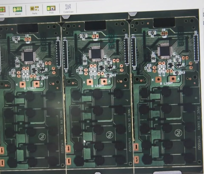
Optical sensor PCB assembly is a manufacturing process that combines precision electronics manufacturing with optical performance control. High-quality products depend not only on PCB design and component performance but also on stable SMT placement, reliable soldering processes, and comprehensive electrical and optical testing.
For applications in industrial control, smart devices, automotive electronics, and other industries, establishing standardized PCB assembly processes is essential for improving the long-term operational reliability of optical sensor products.