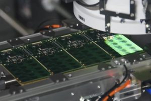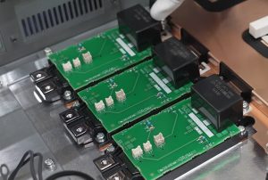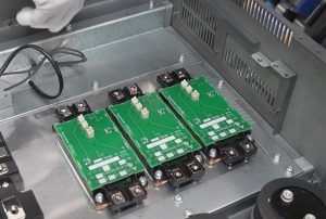

KingTop Technology specializes in PCB assembly for industrial control tablet motherboards, maintaining strict control over SMT placement, soldering processes, and quality inspection to ensure stable and reliable products.
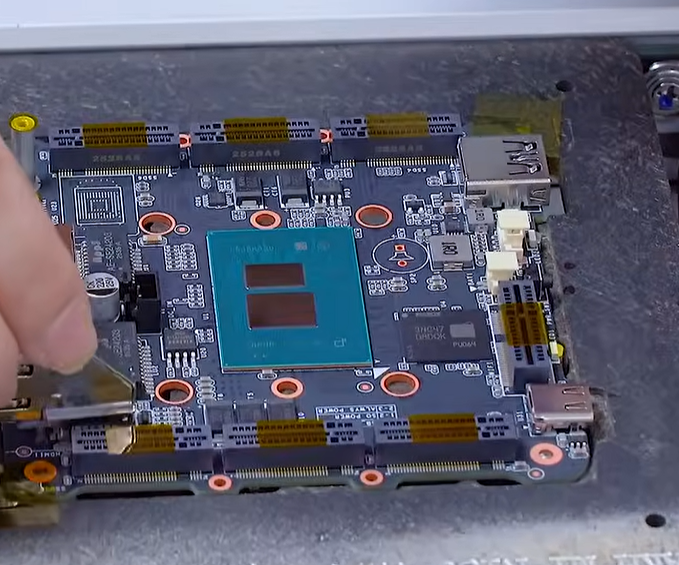
I. Positioning and Requirements for Industrial Panel PC Motherboard PCB Assembly
The motherboard of an industrial panel PC serves as the core control and computing platform for the equipment. It typically handles tasks such as processor operation, storage management, display output, touch interaction, wired and wireless communication, industrial interface control, and power distribution. Compared to consumer electronics, industrial panel PCs operate in more demanding environments—often requiring long-term performance under conditions involving wide temperature ranges, vibration, dust, electromagnetic interference, and continuous power supply.
Consequently, the PCB assembly process for these motherboards cannot merely focus on whether components are soldered onto the board; it must also account for electrical performance, structural fit, thermal design, long-term reliability, and batch-to-batch consistency.
A robust PCB assembly process for industrial panel PC motherboards is driven by product specifications and application requirements, grounded in Design for Manufacturing (DFM) principles, and executed through controlled SMT, through-hole component insertion, soldering, inspection, and verification workflows. Every process parameter must be well-founded, traceable, and verifiable—ensuring that operations do not rely on the subjective, ad-hoc adjustments of individual operators. From a project management perspective, identifying design risks early is far more effective than attempting repairs after the product has reached mass production.
II. Design Documentation and Engineering Preparation Prior to Assembly
2.1 Verification of Documentation Completeness
Before initiating the PCB assembly process for an industrial panel PC motherboard, it is essential to verify all relevant documentation, including schematics, PCB design files, Gerber files, Bills of Materials (BOM), coordinate files (centroid data), assembly drawings, stencil specifications, process requirements, and version history. The BOM must clearly specify material codes, model specifications, component packages, reference designators, and approved brands or authorized alternatives. Coordinate files must be checked for the correct origin, units of measurement, rotation angles, and top/bottom side definitions. Assembly drawings are used to confirm the orientation of connectors, the polarity of specific components, the placement of shielding covers, and any other specialized assembly requirements.
All documentation must be version-synchronized to ensure consistency. In the event of changes to the PCB version, BOM version, or software configuration, an Engineering Change Review must be conducted. This review shall clearly identify the affected materials, stencils, software programs, test fixtures, and the required disposition for work-in-progress (WIP) inventory. Temporary substitute materials that have not been formally validated must not be introduced into full-scale mass production.
2.2 DFM (Design for Manufacturing) Assessment for PCBs and Components
Engineering personnel shall focus on evaluating parameters such as board thickness, layer stack-up, copper weight, surface finish, board-edge processing, panelization, solder mask openings, pad dimensions, and via design. For critical packages—including BGAs, QFNs, fine-pitch connectors, and large-format processors—the review must encompass pad design, stencil aperture specifications, and reflow process conditions. In high-density areas, it is also necessary to verify component spacing, clearance for rework, and accessibility for inspection.
Regarding components, ensure that packages match their corresponding pads, polarity markings are clear, and the supply of critical components remains stable. Furthermore, assess the process implications of mixing components of varying heights, as well as the handling of heat-sensitive parts, connectors, and shielding structures. PCB assembly for industrial control tablet motherboards typically involves CPUs, memory modules, power management ICs, storage devices, interface chips, and wireless communication modules; the packaging, batch traceability, and substitution criteria for these critical components must be strictly controlled.
2.3 Production Process Planning
Based on product architecture and order volume, define the appropriate process flow—such as single-sided or double-sided SMT, through-hole component insertion (THT), selective soldering, manual touch-up, and the application of conformal coatings. Establish, in advance, the requirements for first-article inspection (FAI), critical process parameters, inspection standards, sampling plans, and escalation protocols for anomalies. Any soldering, assembly, or testing issues identified during the trial production phase must be documented in an issue log and tracked to closure; unverified process conditions must not be directly transferred to mass production.
III. Core Process Flow for Industrial Control Tablet Motherboard PCB Assembly
3.1 Incoming Material Inspection and Control
Incoming PCBs must be inspected for physical appearance, warpage, board-edge condition, pad oxidation, damage to the solder mask, and the accuracy of markings (such as labels and version identifiers). Where necessary, verify dimensions, thickness, and electrical performance in accordance with product specifications. Electronic components must be verified for model, package type, quantity, batch, packaging, and traceability information. For moisture-sensitive devices (MSDs), processes such as drying, tracking of open-bag duration, and baking must be managed in accordance with supplier requirements and applicable standards to prevent delamination or the “popcorn effect” during the reflow soldering process.
Solder paste, flux, and cleaning agents must be stored, brought to room temperature, and used within their specified shelf life and under prescribed conditions. Material issuance must follow batch management protocols; all material changes, returns, and the recovery of surplus materials must be documented. The stability of PCB assembly for industrial tablet motherboards depends, first and foremost, on the input materials being authentic, compliant, and traceable.
3.2 Solder Paste Printing
Prior to printing, inspect the stencil apertures, tension, cleanliness, and alignment with the PCB. Ensure that the squeegee, printing pressure, speed, release parameters, and the condition of the solder paste are all properly matched. Following the printing process, use Solder Paste Inspection (SPI) to measure solder volume, area, offset, and height—paying particular attention to fine-pitch pins, BGA pads, QFN thermal pads, and connector pads.
In the event of insufficient solder, bridging, misalignment, or clogged apertures, analyze the stencil, support setup, cleaning frequency, and printing parameters before making adjustments and conducting re-verification.
The quality of solder paste printing directly influences the formation of subsequent solder joints. For industrial tablet motherboard PCB assembly, visual inspection alone is insufficient; for critical pads, SPI data should be used to establish process trends, ensuring that defects do not propagate to the placement and reflow stages.
3.3 SMT Placement
Before placement, verify the accuracy of the placement program, component library, nozzles, feeders, and PCB fiducial marks. The equipment must be configured to recognize component polarity, orientation, and package characteristics. After the first article is processed, perform a detailed check of each component’s reference designator, model, orientation, and placement offset. Establish specific “first article” inspection checkpoints for critical components, such as processors, memory modules, power management ICs, clock devices, and connectors.
For BGA, QFN, and fine-pitch components, particular attention must be paid to controlling placement offset, pressure, and coplanarity. Visual compensation systems on placement equipment cannot replace pre-production verification. If coordinate rotation issues or library file errors are detected, production must be halted to allow for program correction and re-verification of the first article. For the PCB assembly of industrial tablet motherboards, records of program versions and equipment parameters must be maintained to ensure that production across different shifts and batches adheres to the same controlled conditions.
3.4 Reflow Soldering
Reflow temperature profiles should be established based on the solder paste type, PCB thermal capacity, component temperature tolerance, and the thermal distribution across the board. A thermal profiling board (test board) must be used to verify the preheat phase, soak (constant temperature) phase, time above liquidus, and peak temperature. Large copper areas, shielding cans, connectors, and regions with thick copper traces can cause temperature variations; therefore, it is critical to ensure that solder joints with higher thermal mass achieve sufficient wetting, while also preventing sensitive components from being subjected to excessive thermal stress.
During mass production, parameters such as furnace temperature, conveyor speed, nitrogen atmosphere (if applicable), and equipment alarms must be monitored. Any changes to the temperature profile, equipment maintenance, or material substitutions require re-validation in accordance with established procedures. Following reflow, the assembly must be inspected for defects—such as tombstoning, misalignment, bridging, cold/dry joints, solder balls, or component damage—with defect locations correlated against data from the printing and placement stages.
3.5 Through-Hole Component Insertion, Manual Soldering, and Structural Assembly
Industrial tablet motherboards typically feature power sockets, pin headers, terminals, USB ports, network ports, display interfaces, and other industrial-grade connectors. Prior to insertion, verify the orientation, height, polarity, and positioning requirements. During soldering, control the solder volume, temperature, duration, and the final shape of the solder joints to prevent pad lifting, damage to the via/hole walls, or short circuits between adjacent terminals. For large-scale or load-bearing connectors, evaluate both the mechanical fixation and the load-bearing capacity of the solder joints.
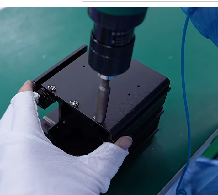
Manual touch-up soldering and rework must be performed using approved process documentation, tools, and temperature ranges. After these operations, inspect the solder joints, surrounding components, and the PCB surface, performing cleaning if necessary. Heat sinks, shielding cans, thermal pads, insulating sheets, and mounting brackets must be installed according to assembly specifications, ensuring correct contact pressure, clearances, and orientation. Care must be taken to avoid board warpage or excessive stress on components resulting from the assembly process. 3.6 Cleaning and Conformal Coating
The necessity of cleaning should be determined based on the type of flux used, the risk posed by residues, the product’s operating environment, and specific customer requirements; cleaning should not be treated as a default step for all products. If cleaning is performed, it is essential to verify the compatibility of the cleaning agent, the coverage of the cleaning process, the effectiveness of the drying stage, and the absence of residues—with particular attention paid to connectors, areas beneath shielding covers, and fine-pitch regions. If a conformal coating (protective coating) is required, the specific areas to be coated, coating thickness, curing conditions, and “no-coat” zones must be clearly defined. Care must be taken to ensure that the coating does not cover connector contacts, test points, thermal contact surfaces, or areas intended for future repair.
IV. Key Quality Control and Defect Prevention
4.1 Process Inspection and Visual Criteria
For the PCB assembly of industrial tablet motherboards, quality checkpoints must be established, including incoming material inspection, solder paste printing inspection, first-article verification, post-reflow inspection, through-hole component inspection, and final inspection. Visual inspection should focus on identifying issues such as incorrect or missing components, reversed orientation, misalignment, “tombstoning,” solder bridging, insufficient solder, cold/weak solder joints, cracked solder joints, pad damage, and contamination. Inspection criteria must be standardized to ensure consistency in how different personnel evaluate the same types of defects.
4.2 AOI and X-Ray Inspection
Automated Optical Inspection (AOI) is effective for identifying visible solder joints and component assembly anomalies, such as incorrect or missing components, misalignment, polarity errors, and certain soldering defects.
Since conventional optical inspection has limitations for components with hidden solder joints (e.g., BGAs), X-ray inspection—or other appropriate methods—should be employed based on risk assessment. Key areas of focus include voids, bridging, misalignment, and the shape of solder balls.
The inspection strategy should be determined by factors such as component package characteristics, failure risks, customer requirements, and historical data, rather than simply maximizing the volume of inspections.
4.3 Analysis of Critical Defects and Closed-Loop Resolution
Common defects include insufficient solder, solder bridging, cold/weak solder joints, BGA soldering anomalies, tilted connectors, reversed components, and surface contamination. During analysis, trace the issue back along the process chain: for insufficient solder, inspect the stencil apertures, solder paste condition, and pad solderability; for solder bridging, check the print volume, component placement offset, and reflow conditions; for “cold” or open solder joints, examine oxidation, coplanarity, the thermal profile, and pad design. For BGA-related anomalies, utilize X-ray inspection, cross-sectioning, or rework analysis to pinpoint the root cause.
Corrective actions must specify the responsible person, completion deadline, verification method, and the affected production batches. For recurring issues, evaluate whether adjustments are required for DFM (Design for Manufacturing) specifications, material requirements, equipment programming, or inspection/control plans. An issue is considered truly closed only after the root cause has been confirmed and the effectiveness of the corrective action has been verified.
V. Electrical Testing and System-Level Verification
5.1 Basic PCBA Testing
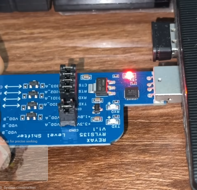
Following the PCB assembly of the industrial tablet motherboard, perform an initial visual inspection and a short-circuit check. Subsequently, in accordance with the test specifications, conduct tests covering power input, standby power consumption, power-rail sequencing, critical voltage and current levels, and protection functions. During the initial power-up, use a current-limited power supply and verify the power rails in the prescribed sequence to prevent secondary damage caused by assembly errors.
5.2 Functional and Interface Testing
Functional testing should encompass processor boot-up, memory recognition, storage read/write operations, display output, touch-interface communication, as well as USB, Ethernet, serial ports, audio, wireless modules, and any customer-specified industrial interfaces. Specific test items should be based on the product configuration; interfaces not included in the configuration should not be subject to mandatory pass/fail criteria. For communication interfaces, verify connection stability, data transfer rates, and data transmission/reception. For display and touch functions, check image quality, brightness control, touch responsiveness, and stability during continuous operation.
5.3 Environmental and Reliability Verification
Based on the product’s intended operating environment, establish verification protocols such as high/low-temperature operation, temperature cycling, vibration, mechanical shock, electrostatic discharge (ESD), electromagnetic compatibility (EMC), and long-term burn-in/aging tests. The test conditions, sample sizes, pass/fail criteria, and post-test inspection requirements must be clearly defined in the verification plan. While environmental verification cannot replace production process control, it is instrumental in identifying potential risks related to thermal design, structural mounting, connector reliability, and power supply margins.
VI. Process Documentation, Traceability, and Mass Production Management
Stable PCB assembly for industrial tablet motherboards requires a comprehensive system of process documentation. This includes Bills of Materials (BOMs) and revision lists, work instructions, equipment programs, reflow profiles, inspection specifications, test specifications, rework procedures, and protocols for handling anomalies.
All documents must be formally approved, and only controlled versions should be used on the production floor. Personnel in critical roles must undergo training and qualification verification. Furthermore, daily management must encompass ESD (electrostatic discharge) control, environmental monitoring (temperature and humidity), equipment checks, and the calibration of jigs and fixtures.
Traceability records must be established for each PCBA (or batch of PCBAs), linking them to at least the following: PCB revision, batches of critical components, production date, equipment or production line used, process parameters, inspection and test results, and any rework history. In the event of a field failure, this allows for the rapid identification of the affected scope and an assessment of risks for the entire batch. For critical components and specialized processes, it is advisable to retain relevant process data and inspection imagery.
Mass production management should also focus on metrics such as the first-pass yield (FPY), overall pass rate, rework rate, scrap rate, and the distribution of primary defects. Data analysis should be categorized by product model, process step, equipment, shift, and material batch to pinpoint the root causes of variability. Simply increasing the number of personnel dedicated to final inspection or rework will not fundamentally improve the quality of industrial tablet motherboard PCB assemblies.
VII. Common Risks and Directions for Engineering Optimization
First, a disconnect between design and manufacturing. Poor design choices—such as improper pad layouts, spacing, panelization, or test point placement—can lead to difficulties in solder paste printing, rework challenges, and “blind spots” during inspection.
A cross-functional DFM (Design for Manufacturing) review, involving R&D, process engineering, quality assurance, and production teams, should be conducted before the PCB design is finalized for production.
Second, inadequate control over the substitution of critical components. Similar physical dimensions do not guarantee identical electrical characteristics, thermal properties, or reliability. Any substitute component must undergo a thorough specification comparison, sample validation, and formal change approval; small-batch trial production should be conducted when necessary.
Third, a lack of validation for process parameters. Parameters for printing, component placement, and reflow soldering should not be based on long-term experience from other product models; instead, they must be determined through validation specific to the actual PCB, component packages, and materials used. Any changes to the process must be evaluated for their impact, and records of these changes must be maintained.
Fourth, insufficient test coverage. Simply confirming that a motherboard can boot up is insufficient to prove that all its interfaces and functions are stable. A test matrix should be established based on product requirements, with clearly defined pass/fail criteria for high-risk interfaces and critical functions.
Fifth, rework management is often inadequate. Repeated heating can damage solder pads, components, and the PCB substrate itself. The number of rework cycles must be limited, and every instance—including the location, reason, method, and outcome—must be documented. For critical solder joints, specialized re-inspection should be performed when necessary.
Conclusion
The PCB assembly of industrial tablet motherboards is a comprehensive system engineering process that integrates engineering design, materials management, SMT placement, precision soldering, quality inspection, and functional verification. The stability and reliability of the final product depend not only on production equipment and assembly techniques but, more importantly, on technical management, process control, and quality traceability throughout the entire lifecycle.
KingTop Technology places great emphasis on every critical stage of the PCB assembly process for industrial tablet motherboards. From initial engineering assessments and Design for Manufacturing (DFM) analysis to SMT placement, reflow soldering, through-hole component assembly, and final product testing, we prioritize the integration of standardized processes, rigorous process control, and thorough quality verification. This approach ensures consistent product quality, enhanced stability, and greater production efficiency.
To meet the stringent requirements for high reliability and long-term, stable operation in the industrial control sector, KingTop Technology remains committed to optimizing PCB assembly processes and improving manufacturing quality. Through professional engineering expertise, rigorous quality management, and standardized production workflows, we provide reliable PCB assembly support for industrial tablet motherboards, helping our clients ensure the stable operation and high-quality delivery of their industrial equipment.